In Situ TEM for Nanomaterial Analysis: Fundamentals, Methods, and Applications in Biomedicine
This article provides a comprehensive overview of in situ Transmission Electron Microscopy (TEM), a transformative technique enabling real-time, atomic-scale observation of nanomaterial dynamics under realistic microenvironmental conditions.
In Situ TEM for Nanomaterial Analysis: Fundamentals, Methods, and Applications in Biomedicine
Abstract
This article provides a comprehensive overview of in situ Transmission Electron Microscopy (TEM), a transformative technique enabling real-time, atomic-scale observation of nanomaterial dynamics under realistic microenvironmental conditions. Tailored for researchers, scientists, and drug development professionals, it covers the foundational principles of in situ TEM, details its methodological approaches including liquid-phase, gas-phase, and heating techniques for nanomaterial synthesis and analysis. It further addresses key challenges and optimization strategies for reliable data acquisition and explores how the technique validates and compares nanomaterial properties and behaviors. By synthesizing insights from foundational to applied research, this guide underscores the critical role of in situ TEM in advancing the rational design and application of nanomaterials, particularly in the biomedical and clinical sectors.
Unlocking the Nanoscale: Core Principles and Capabilities of In Situ TEM
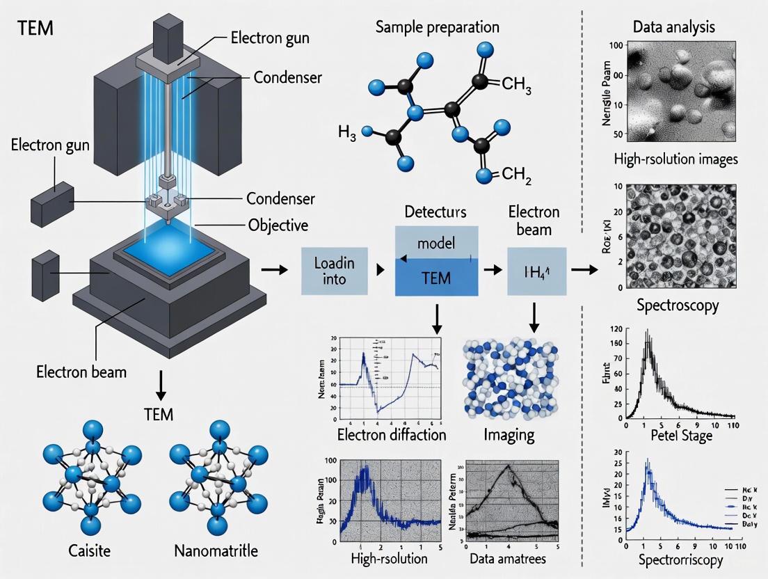
In situ Transmission Electron Microscopy (TEM) has transformed electron microscopy from a tool for static structural analysis into a dynamic platform for observing nanoscale processes in real time. By integrating specialized specimen holders that apply stimuli such as heat, electrical bias, liquid, or gas environments, researchers can now observe material transformations and reactions at atomic resolution under realistic conditions. This technical guide details the fundamental principles, methodologies, and applications of in situ TEM, framing it within the broader context of nanomaterial analysis research. We provide a comprehensive overview of experimental protocols, quantitative data presentation, and essential tools, serving as a critical resource for researchers and scientists advancing frontiers in catalysis, energy storage, and electronic materials.
Transmission Electron Microscopy (TEM) has historically provided unparalleled snapshots of material structure at the atomic level, but traditional approaches are limited by static imaging under high vacuum conditions that do not reflect real-world material operating environments [1]. In situ TEM overcomes this fundamental limitation by enabling real-time observation of a sample's response to an external stimulus within the microscope [2]. This paradigm shift transforms the TEM from a passive observation instrument into an active nanoscale laboratory.
The technique originated in the 1960s when scientists began deliberately modifying materials within the specimen chamber to study electron beam-induced effects, particularly in metals relevant to aviation and space flight [2]. Subsequent advancements in microscope stability, image-capture technology using charge-coupled device (CCD) cameras, and specialized specimen stages have enabled the precise application of stimuli during imaging [2]. Modern in situ TEM now facilitates experiments involving thermal, electrical, mechanical, and chemical stimuli, providing profound insights into dynamic processes across materials science, catalysis, and nanotechnology [3] [4].
Core Principles and Technical Capabilities
Fundamental Operating Principles
In situ TEM maintains the basic operating principles of conventional TEM, where a high-energy electron beam transmits through an electron-transparent sample to generate a projection image or diffraction pattern. The critical innovation lies in integrating specialized holders and micro-electromechanical systems (MEMS) that allow controlled application of external stimuli while maintaining high-resolution imaging capabilities [1]. These systems isolate environmental conditions (liquids or gases) from the microscope's high vacuum using electron-transparent membranes, typically made of silicon nitride, while permitting atomic-scale observation [2].
The temporal resolution of in situ TEM represents a crucial technical parameter. While it enables real-time observation, current limitations exist for processes occurring at nanosecond timescales, which are 6-8 orders of magnitude faster than the microsecond resolution of most in situ TEM systems [2]. This limitation can cause transient phenomena to be blurred or missed entirely, driving ongoing developments in fast-detection technologies.
Stimuli and Environmental Control Capabilities
The experimental versatility of in situ TEM stems from its ability to apply multiple controlled stimuli simultaneously or sequentially. The table below summarizes primary stimulus modalities and their research applications.
Table 1: In Situ TEM Stimulus Modalities and Applications
| Stimulus Type | Technical Implementation | Primary Research Applications | Key Capabilities |
|---|---|---|---|
| Heating | MEMS-based resistive heating chips [5] | Phase transformations, grain growth, thermal stability [6] | Temperatures >1,100°C; double-tilting capability [5] |
| Electrical Biasing | Holders with electrical feedthroughs [7] | Ferroelectric switching, memristive devices, electronic materials [5] [3] | Simultaneous biasing and heating; pA-scale current sensitivity [3] |
| Liquid Environment | Liquid-cell with SiN windows [2] | Nanoparticle growth, electrochemical reactions, biological processes [5] [6] | Static or flow conditions; nanoscale resolution [5] |
| Gas Environment | Microreactor cells with SiN windows [2] | Catalytic reactions, oxidation/reduction, environmental degradation [5] [4] | Pressures up to 2 bar; reactive gas mixtures [5] |
| Mechanical Testing | Actuated holders for nanoindentation [2] | Deformation behavior, fracture processes, mechanical properties [2] | In-situ nanoindentation and compression testing [2] |
Experimental Methodologies and Workflows
General Experimental Framework
Successful in situ TEM experimentation requires meticulous planning and execution across multiple stages. The workflow encompasses sample preparation, holder configuration, stimulus application, and simultaneous data acquisition through multiple detection modalities.
Diagram 1: In Situ TEM Experimental Workflow
Key Experimental Protocols
In Situ Heating Study of Nanomaterial Transformation
The protocol for observing microstructural evolution under thermal stress exemplifies the precise control required for in situ experimentation:
- Sample Preparation: Core-shell Sn@SiO₂ nanoparticles are synthesized via a modified reverse-emulsion method and dispersed onto MEM-based heating chips [6]. Sample dimensions are critical, with typical configurations including 20nm Sn cores with 20nm SiO₂ shells or 30nm cores with 8nm shells [6].
- Holder Configuration: A Protochips Aduro or Dens Solutions Wildfire heating holder is installed, providing double-tilting capability and temperatures exceeding 1,100°C [5].
- Experimental Parameters: Samples are heated from 25°C to 300°C at controlled ramp rates under vacuum conditions. Electron beam conditions are carefully modulated between strong (37.3 pA cm¯²) and weak (2.7 pA cm¯²) intensities to either exploit or minimize beam-induced effects [6].
- Data Acquisition: Dynamic structural changes are recorded using a Gatan OneView CMOS camera at video frame rates (up to 30 fps). Selected Area Electron Diffraction (SAED) patterns are acquired at intervals to identify phase transformations from metallic Sn to SnO₂ [6].
- Key Observations: This protocol enables direct visualization of Sn core liquefaction above 231°C, dynamic movement of Sn nanodroplets within SiO₂ matrices, and subsequent transformation to hollow SnO₂@SiO₂ nanostructures [6].
In Situ Electrical Biasing for Domain Wall Dynamics
The investigation of ferroelectric materials under electrical bias demonstrates the capability for probing electronic and structural properties simultaneously:
- Sample Preparation: Focused ion beam (FIB) milling prepares cross-sectional lamellae of BiFeO₃ thin films. Nanofabrication techniques create electrical contacts on specially-designed chips with electron-transparent Si₃N₄ windows [7] [3].
- Holder Configuration: A Protochips Aduro electrical biasing holder with double-tilt capability is employed, enabling atomic-scale imaging along specific zone axes during electrical stimulation [5] [3].
- Experimental Parameters: Positive ramp biases are applied while maintaining current detection at pA-scale sensitivity. Magnetic fields can be applied perpendicular to the sample plane using the objective lens excitation, with fields calibrated using commercial Hall sensors [7] [3].
- Data Acquisition: Lorentz-TEM imaging visualizes magnetic domain structures, while simultaneous Hall effect measurements monitor transversal voltages. The transport of intensity equation (TIE) reconstruction quantifies in-plane magnetic induction [7].
- Key Observations: This approach reveals the creation and erasure of charged domain walls (CDWs) in BiFeO₃, demonstrating potential applications in ultrahigh-density information storage [3].
The Scientist's Toolkit: Essential Research Reagents and Materials
Implementing successful in situ TEM experiments requires specialized materials and components that enable stimulus application while maintaining imaging capabilities.
Table 2: Essential Research Reagents and Materials for In Situ TEM
| Component | Function | Specific Examples | Technical Specifications |
|---|---|---|---|
| MEMS Chips | Provide platform for applying stimuli while maintaining electron transparency | Protochips Fusion Select chips [7], Dens Solutions Climate chips [5] | SiN windows (200μm edge length) [7]; heating to 1,000°C [5] |
| Specialized Holders | Interface between microscope and sample, delivering stimuli | Protochips Aduro (heating/biasing) [5], Hummingbird (liquid flow) [5] | Double-tilt capability (±15°) [3]; electrical feedthroughs [7] |
| Environmental Cells | Create isolated liquid or gas environments around sample | Protochips liquid/gas cells [2], Bruker cells [2] | Pressure up to 2 bar [5]; controlled gas mixtures [2] |
| Detection Cameras | Capture high-speed, high-resolution temporal data | Gatan K3 IS camera [8], OneView camera [7] | Time resolution: sub-ms [8]; 11520×8184 pixels at 5 fps [8] |
| Analytical Spectrometers | Provide chemical and electronic state information during experiments | Gatan GIF Continuum EELS [8], SDD EDS detectors [7] | Real-time oxidation state quantification [8] |
Technical Considerations and Limitations
Despite its powerful capabilities, in situ TEM introduces several technical challenges that researchers must address experimentally.
Spatial and Temporal Resolution Constraints
The pursuit of atomic resolution remains challenging under certain in situ conditions. Liquid-cell TEM typically achieves resolution limited to a few nanometers due to scattering effects from the liquid layer and confinement windows [5]. Temporal resolution represents another significant constraint, as many transient phenomena in catalysis and materials science occur at nanosecond timescales, while most in situ TEM systems operate effectively at microsecond resolution [2]. This limitation can obscure critical intermediate states in dynamic processes.
Electron Beam Effects
The high-energy electron beam inevitably interacts with samples, potentially inducing artifacts that complicate data interpretation. Beam effects can include radiolysis in liquid samples, heating, knock-on damage in crystalline materials, and even direct chemical reduction [6]. These factors necessitate careful experimental design, including dose-controlled imaging, appropriate control experiments, and comparison with ex situ characterization where possible.
Sample Preparation Complexities
Preparation of electron-transparent samples compatible with in situ holders presents significant challenges. Samples must be thinner than 100nm while maintaining structural integrity and incorporating electrodes or environmental confinement where needed [7] [3]. The complexity of these preparations often requires sophisticated nanofabrication approaches including optical lithography, reactive ion etching, and focused ion beam milling [7].
Future Perspectives and Emerging Directions
The evolution of in situ TEM continues with several promising technological developments. Integration with machine learning and advanced data analysis approaches will enhance the extraction of meaningful information from complex, multi-dimensional datasets [9]. The combination of multiple simultaneous stimuli (e.g., electrical biasing in liquid environments) more closely mimics operational conditions in devices such as batteries and electrocatalysts [5]. Additionally, the development of faster detectors will address current temporal resolution limitations, potentially enabling the observation of previously inaccessible transient phenomena [2] [8].
Table 3: Quantitative Comparison of In Situ TEM Techniques
| Technique | Spatial Resolution | Temporal Resolution | Key Measurement Types | Representative Applications |
|---|---|---|---|---|
| In Situ Heating TEM | Atomic scale [5] | Seconds to minutes [8] | Phase transformation, grain growth, diffusion [6] | Nanoparticle sintering, thermal stability [6] |
| In Situ Liquid-Cell TEM | ~1-2 nm [5] | Video rate (30 fps) [8] | Nucleation & growth, dissolution, corrosion [2] [6] | Nanoparticle synthesis, battery cycling [5] [6] |
| In Situ Gas-Cell TEM | Atomic scale [5] | Seconds to minutes [8] | Surface reconstruction, oxidation/reduction [4] | Catalytic reactions, environmental degradation [5] [4] |
| In Situ Electrical TEM | Atomic scale [3] | Milliseconds to seconds [8] | Domain wall dynamics, resistive switching [3] | Ferroelectric devices, memristive materials [5] [3] |
| In Situ Mechanical TEM | Nanoscale [2] | Video rate (30 fps) [8] | Dislocation dynamics, fracture, deformation [2] | Nanomechanics, irradiation-induced hardening [2] |
In situ TEM represents a revolutionary advancement in microscopy, transforming the TEM from a passive imaging tool into a dynamic experimental platform. By enabling real-time observation of nanomaterial behavior under realistic stimuli, this technique provides unprecedented insights into fundamental processes across materials science, catalysis, and nanotechnology. While technical challenges remain regarding resolution limitations and beam effects, ongoing developments in MEMS technology, detector design, and multi-modal integration continue to expand the capabilities of this powerful methodology. As these advances mature, in situ TEM will play an increasingly critical role in bridging the gap between static nanoscale structure and dynamic material function, accelerating the design and optimization of next-generation nanomaterials for diverse technological applications.
The controllable synthesis of nanomaterials remains a formidable challenge in materials science, primarily due to the inability to observe and understand atomic-scale processes during nucleation and growth. This in-depth technical guide explores how in situ transmission electron microscopy (TEM) bridges this critical knowledge gap. By enabling real-time, atomic-scale visualization of nanomaterial dynamics under various microenvironmental conditions, in situ TEM provides unprecedented insights into the fundamental mechanisms governing nanomaterial synthesis. This review details the operational principles, methodological approaches, and specific applications of in situ TEM in overcoming longstanding hurdles in nanomaterial control, including precise manipulation of size, morphology, crystal structure, and phase evolution. The integration of advanced techniques such as 4D-STEM and machine learning is further pushing the boundaries of quantitative, atomic-scale analysis in nanomaterial research.
Nanomaterials, defined by their size typically ranging from 1 to 100 nanometers, have revolutionized materials science due to their unique properties and broad applications in catalysis, energy, and biomedicine [10]. However, the controlled fabrication of nanomaterials—achieving precise command over their size, shape, crystal structure, and surface properties—presents a complex challenge that is critical for tailoring their performance [10]. Traditional ex situ characterization techniques fall short in capturing the dynamic, atomic-scale processes that govern nanomaterial formation and evolution [11] [10].
In situ transmission electron microscopy (TEM) has emerged as a transformative tool that overcomes these limitations by providing a platform for real-time observation and manipulation of nanostructures with atomic precision [10]. This guide examines how in situ TEM addresses fundamental synthesis hurdles by revealing nucleation events, growth pathways, and structural dynamics as they occur under realistic conditions. We explore the technical methodologies, experimental protocols, and cutting-edge applications that are turning nanomaterial synthesis from an empirical art into a predictable science.
Fundamental Synthesis Challenges in Nanomaterials
The quest for precision in crafting nanomaterials with tailored properties is hindered by multiple fundamental challenges that in situ TEM directly addresses:
Unobserved Nucleation and Growth Mechanisms: The journey from atomic monomers to stable nanocrystals involves complex processes that classical and non-classical nucleation theories cannot fully predict. The reality of atomic migration dynamics, interfacial evolution, and structural transformation during synthesis often deviates significantly from theoretical models [10]. Without direct observation, these mechanisms remain poorly understood.
Control of Size and Morphology: Techniques such as wet chemical synthesis and solid-state reactions often yield nanomaterials with broad size distributions and morphological diversity, compromising their performance in specific applications [10]. The high surface-to-volume ratio of nanomaterials, while responsible for their unique properties, also introduces substantial variability during synthesis.
Environmental Influence and Reproducibility: Environmental factors during synthesis—including temperature, pressure, and the presence of surfactants or solvents—significantly affect crystallinity, phase, and surface properties, leading to challenges in reproducibility [10].
Phase and Structural Stability: Phase transformations and structural changes under different stimuli (thermal, mechanical, or chemical) can alter the intended properties of nanomaterials. For instance, the thermal stability of magnetic nanoparticles is crucial for high-temperature applications, yet phase changes can render them ineffective [10].
Instrumental Foundations of In Situ TEM
Core Principle and Capabilities
In situ TEM combines the high-resolution imaging capabilities of conventional TEM with the application of external stimuli to observe real-time sample dynamics [8]. This approach allows researchers to apply various stimuli including electrical biasing, mechanical deformation, heating, cooling, light illumination, and the introduction of gaseous or liquid environments while simultaneously observing material responses [8]. The spatial resolution can range from tens of nanometers to fractions of an angstrom, with temporal resolutions from seconds to less than a millisecond [8].
Environmental Cell Designs
Two primary designs have been developed to confine reactive environments to the sample region while maintaining high vacuum conditions for the electron gun:
Table 1: Comparison of Environmental TEM Cell Designs
| Cell Type | Operating Principle | Maximum Pressure/Temperature | Key Advantages | Key Limitations |
|---|---|---|---|---|
| Thin-Window Cell | Sealed sample holder with electron-transparent windows isolates gas/liquid from column vacuum [12] | Up to 1 atmosphere; 800-1000°C with MEMS heaters [12] | No TEM modifications required; supports commercial holders [12] | Reduced image contrast/resolution; limited analytical capabilities [12] |
| Differential Pumping System | Multi-stage small apertures above/below sample enable direct gas introduction [12] | ~20 Torr pressure; higher temperature capability [12] | Superior resolution; higher temperature capability; better sample tilting; supports EELS [12] | Requires TEM reconfiguration; lower pressure limits [12] |
Advanced Imaging and Analytical Techniques
Modern in situ TEM incorporates multiple complementary techniques:
- Scanning TEM (STEM): Provides high-resolution imaging with Z-contrast [12] [8]
- Electron Energy-Loss Spectroscopy (EELS): Analyzes chemical composition and bonding states in real-time [12] [8]
- Energy-Dispersive X-ray Spectroscopy (EDS): Enables elemental mapping during experiments [12] [8]
- 4D-STEM: Records diffraction patterns at each scan position using pixelated detectors, revealing crystal orientations, local strain fields, and lattice defects [13]
Experimental Methodologies and Protocols
Gas-Phase Nanomaterial Synthesis
Gas-phase in situ TEM enables direct visualization of oxygen-adsorption-induced reconstructions on metal surfaces, kinetics of oxide nucleation and growth, and morphological evolution of oxide islands in gas environments [12]. The experimental workflow typically involves:
Diagram Title: Gas-Phase TEM Experimental Workflow
Detailed Protocol:
- Sample Preparation: Fabricate thin metal films or nanoparticles on electron-transparent substrates (e.g., SiNₓ membranes) [12].
- Cell Loading: Transfer sample to gas cell holder, ensuring proper sealing of the reaction environment [12].
- Environment Control: Introduce reactive gases (e.g., O₂ for oxidation studies) at controlled pressures (up to 1 atm for window cells, ~20 Torr for differential pumping) [12].
- Real-Time Imaging: Acquire time-resolved high-resolution images, diffraction patterns, and spectroscopic data while maintaining environmental conditions [12] [8].
- Data Analysis: Apply quantitative analysis including particle tracking, diffraction pattern indexing, and spectral analysis to extract kinetic parameters [14].
Liquid-Phase Nanomaterial Synthesis
Liquid-phase TEM (LP-TEM) enables observation of electrochemical reactions, such as metal dissolution, passivation, and oxide formation, under applied potentials or in the presence of corrosive liquids [12]. The methodology includes:
Electrochemical Liquid Cell Protocol:
- Cell Assembly: Fabricate liquid cell with two electron-transparent windows (typically SiNₓ), patterned electrodes, and spacer layers to create a thin liquid cavity (<1 µm) [12] [13].
- Solution Introduction: Inject precursor solutions (e.g., 5 mM CuSO₄ with 5 mM KCl for copper electrodeposition) into the liquid cell [13].
- Potential Control: Apply controlled potentials (e.g., cyclic voltammetry from -0.17 V to oxidizing potentials) using integrated microelectrodes [13].
- 4D-STEM Data Acquisition: Acquire nanobeam scanning electron diffraction datasets with pixelated detectors to obtain structural and crystallographic information [13].
- Phase Mapping: Use virtual off-axis dark-field imaging reconstructed from 4D-STEM data to map phase distribution (e.g., Cu vs. Cu₂O) within nanoparticles [13].
The Scientist's Toolkit: Essential Research Reagents and Materials
Table 2: Key Research Reagent Solutions for In Situ TEM Experiments
| Item | Function/Application | Specific Examples |
|---|---|---|
| SiNₓ Membrane Windows | Electron-transparent containment for liquid/gas environments [12] | 10-50 nm thick windows for liquid cells; support pressures up to 1 atmosphere [12] |
| MEMS-based Heaters | High-temperature sample control in windowed cells [12] | Enable operation at 800-1000°C during gas-phase reactions [12] |
| Electrochemical Precursors | Metal ion sources for nucleation and growth studies [13] | 5 mM CuSO₄ + 5 mM KCl for copper electrodeposition studies [13] |
| Graphene Liquid Cells | High-resolution liquid imaging with minimal electron scattering [12] | Single-atom-thick graphene layers encapsulating liquid solutions [12] |
| Pixelated Detectors | 4D-STEM data acquisition for structural analysis [13] | Enable recording of full diffraction patterns at each scan position in liquid [13] |
Addressing Specific Nanomaterial Synthesis Challenges
Unveiling Nucleation and Growth Mechanisms
In situ TEM has fundamentally transformed our understanding of nucleation and growth processes by directly visualizing previously theoretical concepts:
Oxide Nucleation in Gas Environments: E-TEM enables direct observation of oxygen-adsorption-induced reconstructions on metal surfaces, revealing that oxidation begins with dissociative chemisorption of molecular oxygen, followed by nucleation, growth, and coalescence of oxide islands that ultimately form a continuous oxide layer [12]. These processes are influenced by intrinsic metal properties (crystal orientation, surface structure, defects) and external factors (oxidizing gases, pressure, temperature) [12].
Electrochemical Nucleation in Liquid: LP-TEM reveals heterogeneous nucleation during electrodeposition, showing considerable variation in particle size even at identical deposition potentials due to heterogeneous electrode properties and ohmic drops [13]. 4D-STEM further identifies that electrodeposited copper nanoparticles contain planar faults (twins, stacking faults) and nanocrystalline structures resulting from coalescence of differently oriented particles or layer-by-layer growth [13].
Controlling Size, Morphology, and Crystal Structure
The real-time observation capabilities of in situ TEM enable researchers to correlate synthesis parameters with resulting nanomaterial characteristics:
Morphological Evolution Tracking: In situ LP-TEM with 4D-STEM has visualized the dynamic electrodeposition of Cu nanoparticles and their subsequent oxidation-induced hollowing, revealing how applied potentials and solution conditions determine final particle morphology [13].
Crystal Structure Control: Virtual bright-field and dark-field imaging reconstructed from 4D-STEM data enables mapping of crystal orientation distributions and identification of planar defects within faceted nanoparticles, providing insights for controlling crystallographic characteristics [13].
Phase Transformation Monitoring: The coexistence of Cu⁰ and Cu⁺ in copper-based electrocatalysts synergistically promotes CO dimerization in CO₂RR. In situ TEM with 4D-STEM enables mapping of phase distribution within partially oxidized nanoparticles, crucial for understanding and optimizing their catalytic performance [13].
Technical Approaches for Specific Nanomaterial Classes
Diagram Title: In Situ TEM Techniques for Nanomaterials
Table 3: In Situ TEM Solutions for Nanomaterial Synthesis Challenges
| Synthesis Challenge | In Situ TEM Approach | Revealed Mechanisms |
|---|---|---|
| Uncontrolled Nucleation | Liquid-cell TEM with electrochemical control | Heterogeneous nucleation sites; size variation due to electrode properties and ohmic drops [13] |
| Irregular Morphologies | Time-resolved STEM imaging during growth | Dynamic shape evolution influenced by solution conditions and applied potentials [13] |
| Unpredictable Phase Transformations | 4D-STEM with phase mapping | Distribution of metallic and oxide phases within composite nanoparticles [13] |
| Defect Formation | Nanobeam electron diffraction in liquid | Identification of planar faults (twins, stacking faults) in faceted nanoparticles [13] |
| Oxidation Dynamics | Gas-phase ETEM with atomic-resolution imaging | Oxide island nucleation, growth, and coalescence mechanisms [12] |
Current Limitations and Future Perspectives
Despite its transformative impact, in situ TEM faces several challenges that represent opportunities for future development:
Spatial and Temporal Resolution Trade-offs: Maintaining atomic resolution while capturing rapid dynamic processes remains challenging, particularly in liquid environments where electron scattering degrades resolution [13]. Future developments in detector technology and beam control promise to enhance these capabilities.
Electron Beam Effects: The incident electron beam can cause unintended sample transformations, including particle growth, rotation, dissolution, and redeposition, potentially altering natural processes [13]. Advanced low-dose imaging techniques and careful control of beam conditions are essential to minimize these artifacts.
Environment Representation: Thin liquid layers in LP-TEM may deviate from bulk conditions due to larger ohmic drops, diffusion limitations, and mass-transport restrictions, particularly in electrochemical reactions governed by mass transport [13]. The introduction of gas bubbles to reduce liquid thickness creates additional gas-liquid interfaces that can alter surface properties [13].
Data Analysis Complexity: The massive datasets generated by in situ TEM, particularly from 4D-STEM and time-resolved experiments, require advanced analysis methods. Emerging approaches include deep learning-based digital twins of experiments for extracting spatio-temporal information from dynamic processes [14].
Future developments will likely focus on the integration of machine learning algorithms for automated data analysis, improved environmental control for more realistic condition replication, and the combination of multiple characterization techniques within a single experiment for comprehensive material analysis [11] [10].
In situ TEM has fundamentally transformed our approach to nanomaterial synthesis by providing unprecedented atomic-scale visualization of dynamic processes during nucleation, growth, and phase evolution. By bridging critical knowledge gaps across different stages of material formation, this powerful methodology enables researchers to move beyond empirical optimization toward rational design of nanomaterials with precisely controlled properties. As technical capabilities continue to advance—particularly through integration with 4D-STEM, machine learning, and enhanced environmental control—in situ TEM is poised to unlock new frontiers in nanomaterial science, enabling the development of next-generation materials for catalysis, energy storage, electronics, and biomedical applications. The atomic-scale insights provided by this technique are not only overcoming longstanding synthesis hurdles but are also paving the way for predictive nanomaterial design with tailored functionalities for specific technological applications.
Transmission Electron Microscopy (TEM) has established itself as an indispensable technique for visualizing matter at the atomic scale. Achieving sub-ångström (<1 Å) resolution represents a fundamental capability for probing the intrinsic properties of nanomaterials, enabling researchers to understand the connections between atomic-scale structure and macroscopic properties and performance [15] [16]. This technical guide examines the core principles and advanced methodologies that push resolution beyond the 1 Å barrier, with particular emphasis on its application within in situ TEM for nanomaterial analysis. The evolution from conventional high-energy TEM to innovative, lower-voltage platforms coupled with computational techniques is redefining the limits of what is observable, providing nanomaterial scientists and drug development professionals with unprecedented analytical power.
The Fundamental Instrumentation for Sub-Ångström Imaging
The pathway to sub-ångström resolution is governed by the microscope's instrumental components and the fundamental physics of electron-sample interactions. The key elements include the electron source, lens system, and detectors, all operating within an ultra-high vacuum environment to eliminate electron beam scattering by gas molecules [16].
Electron Guns and Coherence
The electron source is the origin of both the beam's resolution potential and its limitations. The brightness, spatial coherence, and temporal coherence of the source are paramount [16]. Field Emission Guns (FEGs), particularly Cold FEGs, provide the highest performance for sub-ångström work, offering exceptional brightness and minimal energy spread, which directly enhances temporal coherence [16]. The temporal coherence length (λc) is given by λc = v h/ΔE, where v is electron velocity, h is Planck’s constant, and ΔE is the energy spread of the beam. A smaller ΔE results in a longer coherence length, improving resolution [16].
Table: Characteristics of Electron Sources for High-Resolution TEM
| Source Type | Crossover Size (nm) | Brightness (A/m²sr) | Energy Spread at 100 kV (eV) | Typical Application |
|---|---|---|---|---|
| Tungsten (Thermionic) | >10⁵ | 10¹⁰ | 3.0 | Conventional TEM |
| LaB₆ (Thermionic) | 10⁴ | 5 x 10¹¹ | 1.5 | High-Resolution TEM |
| Schottky FEG | 15 | 5 x 10¹² | 0.7 | Sub-Ångström S/TEM |
| Cold FEG | 3 | 10¹³ | 0.3 | Ultra-High Resolution S/TEM |
The Role of Accelerating Voltage
The electron wavelength (λ) is inversely related to the accelerating voltage (V) through the de Broglie relation. Higher voltages (e.g., 300 kV) yield shorter wavelengths, theoretically enabling higher resolution [16] [17]. However, recent breakthroughs demonstrate that with advanced techniques like ptychography, sub-ångström resolution is achievable even at intermediate (200 kV) and low (20 keV) voltages [15] [18] [17]. Lower voltages offer the advantage of increased elastic scattering cross-sections, providing greater image contrast for thin, light-element samples such as 2D materials and biological macromolecules [15].
Table: Achieved Resolution at Various Accelerating Voltages
| Accelerating Voltage | Achieved Resolution | Key Technique | Sample | Source |
|---|---|---|---|---|
| 300 kV | < 1.0 Å | Conventional AC-TEM | Various | [15] |
| 200 kV | ~1.6 Å | Single-Particle Cryo-EM | Apoferritin | [17] |
| 80 kV | Sub-Ångström | Ptychography | TMDCs | [15] |
| 20 keV | 0.67 Å | Multi-slice Ptychography | Not Specified | [15] |
Advanced Imaging: Electron Ptychography
Ptychography has emerged as a revolutionary computational imaging technique that bypasses the hardware limitations of conventional TEM, enabling deep-sub-ångström resolution even on simpler, lower-cost microscope platforms [15] [18].
Core Principles and Workflow
Ptychography operates by acquiring a grid of convergent-beam electron diffraction patterns from a large number of small, overlapping illumination areas on the sample [15]. A computational algorithm, such as the extended ptychographical iterative engine (ePIE), then iteratively solves for the complex wave function exiting the sample (specimen transmission function) and the precise probe function, creating a quantitative model of the amplitude and phase shift imposed by the sample [15]. The phase shift information is particularly valuable as it often contains superior contrast compared to conventional imaging.
Methodologies for High-Resolution Ptychography
The experimental protocol for achieving sub-ångström resolution via ptychography involves several critical steps:
- Instrument Setup: The microscope must be equipped with a coherent electron source (e.g., cold FEG) and a hybrid pixelated direct detector optimized for high dynamic range and high-speed acquisition of diffraction patterns [15].
- Data Acquisition: A 2D diffraction pattern is recorded at each probe position in a 2D raster scan. For 0.67 Å resolution, electrons scattered up to ~10 degrees (~175 mrad) must be captured, requiring a detector with a large enough collection angle [15].
- Data Pre-processing: This includes distortion correction (e.g., for pincushion distortion from projector lenses) and potentially energy filtering to remove inelastically scattered electrons, which is crucial for imaging thick samples (up to 85 nm) [15] [18].
- Computational Reconstruction:
- Algorithm Selection: For thin samples, the ePIE or similar single-slice algorithm may suffice. For thicker samples where the electron wave undergoes multiple scattering, a multi-slice ptychography algorithm must be employed to accurately model the propagation through different sample depths [15] [18].
- Advanced Refinements: The highest resolutions are achieved by incorporating diffraction distortion correction and, for very thick objects, an extended local-orbital ptychography (eLOP) that can retrieve and correct for probe aberrations that vary during scanning [15] [18].
Electron-Sample Interactions and Information Transfer
The interaction between the high-energy electron beam and the thin specimen is the source of contrast and information in TEM, but it also imposes fundamental limits.
The Contrast Transfer Function (CTF)
The CTF is a mathematical description of how the electron microscope's optics and aberrations modify the image information from the sample [19]. It is an oscillating function that dictates which spatial frequencies (and thus which details) are faithfully transferred or inverted and suppressed in the final image. Accurate CTF estimation and correction are essential for achieving the microscope's theoretical information limit [19].
Optimizing Information at Low Voltages
For light-element nanomaterials and biological specimens, the trade-off between radiation damage and information transfer is critical. The information coefficient (ζ) is defined as ζ = T(σe/σi), where T is the total electron transmission through the sample, σe is the elastic scattering cross-section, and σi is the inelastic scattering cross-section [15]. This coefficient is optimized at lower beam energies (≤ 30 keV) as the sample thickness is reduced (e.g., to ≤ 15 nm for carbon-based materials). At these lower energies, the increased elastic scattering provides better contrast, which can outweigh the effects of increased damage for suitably thin samples [15]. This principle is vital for in situ studies of sensitive nanomaterials like MoS₂ and for the structural determination of small proteins (<100 kDa) in cryo-EM [15].
The Scientist's Toolkit: Essential Research Reagents and Materials
Table: Key Instrumental and Computational "Reagents" for Sub-Å TEM
| Item / Solution | Function / Role | Technical Specification / Example |
|---|---|---|
| Cold Field Emission Gun (FEG) | Provides high-brightness, coherent electron source for high-resolution imaging. | Brightness ~10¹³ A/m²sr, energy spread ~0.3 eV [15] [16]. |
| Hybrid Pixelated Direct Detector | Records high-dynamic-range, high-speed 2D diffraction patterns for ptychography. | Optimized for low-energy electrons; enables fast 4D-STEM acquisition [15]. |
| Immersion Objective Lens | Provides strong focusing of the electron probe onto the sample. | Key component in achieving a small, stable probe for scanning diffraction [15]. |
| Multi-Slice Ptychography Algorithm | Computational engine to reconstruct sample's electrostatic potential from 4D dataset. | Models multiple scattering in thick samples; essential for >~30 nm samples [15] [18]. |
| Extended Local-Orbital Ptychography (eLOP) | Advanced algorithm correcting for residual and varying probe aberrations. | Enables high-precision imaging of very thick objects (e.g., 85 nm Si) [18]. |
| Energy Filter | Removes inelastically scattered electrons to improve contrast and signal-to-noise. | Critical for achieving an 18 pm information limit in thick samples [18]. |
The frontier of sub-ångström resolution in TEM is being advanced by a synergy of sophisticated hardware and computational microscopy. The demonstration of 0.67 Å resolution at 20 keV and the precise imaging of samples up to 85 nm thick signify a paradigm shift [15] [18]. These techniques, particularly ptychography, are making atomic-resolution analysis more accessible and are uniquely suited for in situ studies due to their robustness to certain instabilities and their quantitative output. For the field of nanomaterial analysis, this instrumental core provides the foundation for directly observing intrinsic structural and physical phenomena in solids, from catalyst nanoparticles and battery materials to semiconductor devices, enabling true bottom-up engineering and discovery.
In situ and operando (scanning) transmission electron microscopy [(S)TEM] has emerged as a powerful platform for investigating materials behavior under a variety of stimuli and environmental conditions [20]. This technique combines nanoscale spatial resolution with eV-to-meV energy resolution and adaptable temporal resolution, enabling researchers to observe the structural and chemical evolution of material features including grains, interfaces, surfaces, and defects in real time [20]. The true power of this approach lies in the strategic integration of multiple characterization techniques—imaging, diffraction, and spectroscopy (EDS/EELS)—applied simultaneously while subjecting samples to controlled stimuli. This multimodal methodology provides a comprehensive understanding of structure-property relationships in materials that cannot be fully captured through any single technique alone.
The fundamental advantage of in situ TEM lies in its ability to apply various external stimuli to samples while collecting data, unlocking the potential to evaluate dynamics during electrical biasing, mechanical strain and deformation, heating, cooling, light illumination, and the introduction of gaseous or liquid environments [8]. With modern advancements, these experiments can now encompass much more than just TEM imaging, incorporating techniques such as scanning transmission electron microscopy (STEM) imaging, diffraction, electron energy loss spectroscopy (EELS), energy-dispersive X-ray spectroscopy (EDS), and 4D STEM, all acquired continuously while varying stimuli [8]. This integrated approach allows for deeper insights into the dynamics of the structure, composition, and bonding of materials, providing a more complete picture of material behavior under realistic conditions.
Table 1: Core Techniques in Multimodal TEM Analysis
| Technique | Primary Function | Key Information Obtained | Spatial Resolution |
|---|---|---|---|
| HR-TEM/STEM | Atomic-scale imaging | Crystal structure, defects, interfaces, morphology | <1 Å [20] |
| EELS | Elemental & electronic analysis | Chemical bonding, oxidation states, electronic properties [21] [22] | Atomic-scale [20] |
| EDS | Elemental composition | Elemental mapping, quantitative composition [22] | Atomic-scale [20] |
| Diffraction | Crystal structure analysis | Phase identification, crystal orientation, strain | Varies by modality |
Fundamental Principles of Integrated Techniques
Electron Energy-Loss Spectroscopy (EELS) Fundamentals
Electron energy-loss spectroscopy operates on the principle of measuring the energy distribution of electrons that have undergone inelastic scattering when transmitting through a thin specimen [21]. In a TEM or STEM, a beam of electrons accelerated to energies between 100 keV and 1 MeV interacts with a thin sample (typically less than 50 nm thickness), and the EELS technique focuses specifically on the inelastic interactions between the primary beam electrons and the electrons from the sample [21]. The energy loss spectrum is divided into distinct regions, each providing different types of information about the sample.
The EEL spectrum is typically divided into three main regions: the zero-loss peak, the low-loss region, and the core-loss region. The zero-loss peak at 0 eV contains all primary electrons that did not undergo noticeable energy loss during transmission, and its width defines the energy resolution of the EELS experiment [21]. The low-loss region (approximately 0-100 eV) is dominated by plasmon peaks and collective oscillations of valence electrons, which can be used to determine the dielectric response of the material via Kramers-Kronig analysis [21]. The core-loss region (above 100 eV) contains element-specific core excitations caused by the excitation of atomic core-states to unoccupied higher energy states, enabling sensitive discrimination between different elements [21].
For chemical quantification, the probability of an inelastic core excitation is given by the cross-section σa, which relates the number of counts in a chosen energy range of the core-excitation edge to the number of atoms of a particular element in the interaction volume [21]. This relationship enables researchers to determine chemical concentrations from EEL spectra, with particular sensitivity to light elements that are problematic in EDX spectroscopy [21].
Energy-Dispersive X-ray Spectroscopy (EDS) Fundamentals
Energy-dispersive X-ray spectroscopy provides complementary elemental and phase analysis at the atomic scale through a different physical mechanism [22]. When the electron beam hits a material, it generates characteristic X-rays that are unique to each element. An EDS detector records these X-rays to produce a spectrum revealing the sample's elemental composition at the position where the electron interaction occurred [22]. This technique has advanced to provide both qualitative and quantitative insights into chemical components, with modern systems combining multiple EDS detectors and utilizing unique windowless detectors for reliable quantitative analysis regardless of atomic number [22].
The combination of EELS and EDS within a single experiment provides a powerful synergy for comprehensive materials characterization. While EELS excels at detecting light elements and providing information about electronic structure and bonding, EDS offers robust quantitative analysis across a wider range of elements and is particularly valuable for heavier elements. When these spectroscopic techniques are integrated with high-resolution imaging and diffraction, researchers obtain a complete picture of both the structural and chemical evolution of materials under various stimuli.
Experimental Design and Workflow
Integrated Data Acquisition Workflow
The successful execution of multimodal in situ TEM experiments requires careful planning and a systematic approach to data acquisition. The general workflow begins with defining the research question and identifying the specific material behaviors to be investigated, which then drives the selection of appropriate stimuli and environmental conditions [20]. Following this, researchers must design the experiment to optimize the collection of imaging, diffraction, and spectroscopic data in a coordinated manner that captures the dynamic processes of interest.
Sample Preparation and Experimental Design Considerations
Sample preparation forms the critical foundation for successful multimodal TEM analysis, requiring substantial experience and skill [22]. The choice of specimen geometry must be optimized for the specific in situ or operando experiment, with various standard starting sample types regularly prepared for (S)TEM analysis [20]. Focused ion beam (FIB) lift-out has become an indispensable technique for preparing site-specific specimens, enabling direct characterization of buried interfaces and structures in heterogeneous systems and devices [20]. Thermo Scientific FIB-SEM instruments, for example, are designed to simplify and speed up TEM sample preparation through specialized software and automation algorithms [22].
When designing multimodal experiments, several critical factors must be considered: (1) what type of data will be required (imaging, diffraction, and/or spectroscopy), (2) how the sample will be prepared, (3) how the electron beam may interact with the sample, (4) how the beam-sample interaction may be affected by the applied stimulus, (5) how reproducible the results may be, (6) whether the results are representative, and (7) how the data will be analyzed and interpreted [20]. For questions requiring access to specifically defined sites such as grain boundaries and interfaces, it is necessary to employ site-specific specimen preparation techniques or use starting materials designed to contain the features of interest in the area being probed [20].
Table 2: Sample Preparation Techniques for Multimodal TEM
| Preparation Method | Best For | Key Considerations | Limitations |
|---|---|---|---|
| FIB Lift-out | Site-specific analysis, buried interfaces, devices | Enables precise targeting of features; modern systems offer automation [22] | Potential for ion beam damage; requires expertise |
| Electropolishing | Bulk metallic samples, uniform thinning | Produces large electron-transparent areas | Limited site-specificity |
| Ultramicrotomy | Soft materials, polymers, biological samples | Can produce serial sections for 3D analysis | Can induce mechanical deformation |
| Drop-casting | Nanoparticles, colloidal suspensions | Simple and rapid preparation | Limited control over particle distribution |
Technical Protocols for Integrated Analysis
Combined EELS/EDS Spectrum Imaging Protocol
The simultaneous acquisition of EELS and EDS data provides complementary chemical information that enhances the reliability of material characterization. This protocol outlines the steps for coordinated EELS/EDS spectrum imaging, which enables correlation of electronic structure information from EELS with elemental composition from EDS.
Specimen Preparation: Prepare a thin specimen (<50 nm thickness for optimal EELS signals [21]) using FIB lift-out or other appropriate methods. Ensure the sample region of interest is electron-transparent and representative of the material system being studied.
Microscope Configuration:
- Align the TEM/STEM for optimal probe formation, using an X-CFEG electron source for high energy resolution in EELS [22]
- Calibrate the EELS spectrometer, noting the full-width at half-maximum of the zero-loss peak defines energy resolution [21]
- Position EDS detectors to maximize solid angle for efficient X-ray collection [22]
Data Acquisition Parameters:
- Set acquisition time per pixel to 0.1-1.0 seconds, balancing signal-to-noise with beam sensitivity
- Define energy ranges: 0-100 eV for low-loss EELS, and specific core-loss edges for elemental analysis [21]
- Configure EDS acquisition to collect full X-ray spectrum (0-20 keV typically)
- Synchronize EELS and EDS acquisition using automatic synchronization tools [8]
Spatial Mapping:
- Define scan area with 64×64 to 256×256 pixels, depending on required spatial resolution and acquisition time constraints
- Set pixel size to 0.1-1 nm based on features of interest
- Acquire simultaneous EELS and EDS spectrum images while maintaining constant beam conditions
Data Processing:
- For EELS: Remove dark current and readout noise, align spectra to account for energy drift
- Apply power-law background subtraction for core-loss EELS analysis [21]
- Perform multiple scattering deconvolution using low-loss spectrum [21]
- For EDS: Apply background subtraction and peak deconvolution for overlapping X-ray lines
- Generate quantitative elemental maps using standardless or standards-based quantification
Data Correlation:
- Register EELS and EDS elemental maps to account for any spatial shifts
- Calculate elemental ratios using both techniques for validation
- Correlate EELS fine structure with local composition from EDS
In Situ Heating with Multimodal Data Collection Protocol
This protocol describes methodology for studying structural and chemical evolution during thermal treatment using combined imaging, diffraction, and spectroscopy.
Holder Preparation and Calibration:
- Select MEMS-based heating holder capable of atomic-resolution imaging at elevated temperatures [22]
- Calibrate temperature measurement using known phase transition materials
- Verify thermal stability across temperature range of interest
Experimental Setup:
- Mount specimen on heating chip using nanomanipulator
- Establish electrical connections and check resistance measurements
- Align TEM for simultaneous imaging, diffraction, and spectroscopy acquisition
Temperature Ramp Procedure:
- Begin at room temperature, acquire reference dataset (imaging, diffraction, EELS, EDS)
- Set heating rate to 1-10°C/minute, depending on process kinetics
- Acquire data continuously or at specific temperature intervals
- For the in-situ upgrade to the GIF Continuum, spectrum images can be acquired at a rate of 1 every 5 seconds, or about 1 every 2°C, during heating [8]
Multimodal Data Acquisition:
- Imaging: Acquire TEM/STEM images at each temperature point
- Diffraction: Record selected area or nanobeam diffraction patterns
- EELS: Collect low-loss and core-loss spectra at identical locations
- EDS: Acquire elemental maps or point spectra synchronized with EELS
Real-time Analysis:
- Monitor changes in crystal structure through live Fourier analysis of images
- Track chemical shifts using real-time EELS quantification of oxidation state [8]
- Observe phase transitions through diffraction pattern evolution
Post-experiment Processing:
- Correlate structural changes with chemical evolution
- Determine activation energies for observed processes
- Create time-temperature-transformation diagrams based on multimodal data
Data Analytics and Interpretation
Multimodal Data Correlation Framework
The integration of imaging, diffraction, and spectroscopic data requires sophisticated analytical approaches to extract meaningful structure-property relationships. The massive datasets generated by in situ multimodal TEM experiments, which can reach terabyte scales, necessitate high-throughput methods and robust computational resources [20]. Modern data analytics for multimodal TEM involves several key steps: data preprocessing and alignment, feature identification and tracking, quantitative parameter extraction, and correlation across techniques.
A critical aspect of multimodal data interpretation involves recognizing the complementary strengths and limitations of each technique. For example, EELS provides exceptional sensitivity to light elements and detailed information about electronic structure through energy loss near-edge structure (ELNES) and extended energy-loss fine structure (EXELFS) [21], while EDS offers more straightforward quantification for heavier elements and is less affected by thickness variations [22]. Similarly, imaging reveals morphological and structural changes, while diffraction provides quantitative information about crystal structure, strain, and phase distributions. By correlating information from all these techniques, researchers can develop comprehensive models of material behavior under various stimuli.
Table 3: Analytical Capabilities of Integrated TEM Techniques
| Analysis Type | Primary Technique | Complementary Technique | Information Gained |
|---|---|---|---|
| Oxidation State | EELS (ELNES) [21] | EDS (elemental ratios) | Chemical bonding, valence states [21] |
| Phase Identification | Electron Diffraction | STEM Imaging | Crystal structure, phase distribution |
| Elemental Mapping | EDS (quantitative) [22] | EELS (light elements) [21] | Comprehensive elemental distribution |
| Interface Analysis | HR-STEM (atomic structure) | EELS/EDS (chemical gradients) | Structure-composition relationships at interfaces |
| Defect Chemistry | TEM/STEM (defect imaging) | EELS (local electronic structure) | Defect identity and influence on properties |
Data Processing Workflows and Visualization
Effective data processing workflows are essential for extracting maximum information from multimodal TEM experiments. The following diagram illustrates the integrated data processing pipeline for correlating information across techniques:
The data processing workflow begins with essential preprocessing steps including drift correction, noise reduction, spatial alignment, and spectral processing [8]. For EELS data specifically, this includes power-law background subtraction and multiple scattering removal [21]. Following technique-specific analysis, the core of multimodal analysis lies in correlating information across techniques through multivariate analysis and multi-parameter visualization, ultimately leading to mechanistic interpretation of observed phenomena.
Essential Research Tools and Materials
The successful implementation of multimodal TEM analysis requires access to specialized instrumentation, holders, and analytical tools. The research toolkit can be divided into several categories: microscope systems, specimen holders, detectors, and analytical software. Each component must be selected and optimized for the specific requirements of integrated imaging, diffraction, and spectroscopy experiments.
Table 4: Essential Research Toolkit for Multimodal TEM
| Tool Category | Specific Tools | Key Features | Application in Multimodal Studies |
|---|---|---|---|
| Microscope Platform | Thermo Scientific Talos (S)TEM [22] | X-CFEG electron source, multiple EDS detectors | High-energy-resolution EELS, simultaneous EDS acquisition |
| In Situ Holders | MEMS-based heating holders [22], Gas/Liquid cells [20] | Atomic-resolution at elevated temperatures, environmental control | Study of material dynamics under realistic conditions |
| Detection Systems | Gatan K3 IS camera [8], Windowless EDS detectors [22] | High-speed acquisition, high detective quantum efficiency | Low-dose imaging, efficient X-ray collection for light elements |
| Spectroscopic Systems | Gatan GIF Continuum [8], EEL spectrometers | Real-time EELS quantification, high energy resolution | Oxidation state mapping, chemical bonding analysis |
| Software Solutions | Velox Software [22], AutoTEM [22] | Automated data acquisition, DPC-STEM, particle analysis | High-throughput experimentation, streamlined workflow |
The selection of appropriate tools must be guided by the specific research questions being addressed. For example, the study of beam-sensitive materials requires cameras like the Gatan K3 IS that can achieve high-resolution imaging at low dose rates [8], while investigations of electronic structure benefit from monochromated sources and high-resolution EELS spectrometers [20]. Similarly, the choice between different in situ holders depends on whether thermal, electrical, mechanical, or environmental stimuli are most relevant to the material system and phenomena under investigation [20].
The integration of imaging, diffraction, and spectroscopy (EDS/EELS) within in situ TEM represents a powerful paradigm for comprehensive materials characterization. This multimodal approach enables researchers to establish direct correlations between structural evolution, chemical composition, and electronic properties under dynamic conditions, providing unprecedented insights into structure-property relationships at the nanoscale. The technical protocols and methodologies outlined in this work provide a framework for designing and executing integrated experiments that leverage the complementary strengths of each technique.
As TEM technology continues to advance, several emerging trends promise to enhance the capabilities of multimodal analysis. The development of faster, more sensitive detectors will enable higher temporal resolution and improved signal-to-noise ratios, particularly for spectroscopic techniques [8]. Increased automation through software solutions like AutoTEM [22] will make complex multimodal experiments more accessible and reproducible. Furthermore, the integration of machine learning and artificial intelligence approaches will help manage and interpret the massive datasets generated by these experiments [20], extracting subtle correlations that might escape conventional analysis. Together, these advancements will further establish multimodal TEM as an indispensable tool for unraveling the complex behavior of materials across diverse fields from energy storage to quantum materials to biological systems.
A Practical Toolkit: Methodologies and Applications of In Situ TEM in Nanosynthesis
Transmission Electron Microscopy (TEM) has evolved from a tool for observing static microstructures into a dynamic platform for investigating material transformations in real time. In situ Transmission Electron Microscopy (in situ TEM) is a advanced characterization technique that combines the high-resolution imaging capabilities of TEM with the application of external stimuli, enabling researchers to observe and analyze the real-time behavior of materials under controlled environments and physical stresses [8]. This methodology allows scientists to bridge the critical gap between a material's static structure and its dynamic functional properties, providing unprecedented insights into atomic-scale processes during chemical reactions, phase transformations, and mechanical deformation.
The fundamental principle underlying in situ TEM involves integrating specialized specimen holders that apply various stimuli—including heat, electrical fields, liquid environments, gaseous atmospheres, or mechanical stress—while the sample is under the electron beam [5]. This capability has transformed our understanding of materials across diverse fields including catalysis, energy storage, electronics, and nanotechnology. By observing processes as they occur rather than inferring mechanisms from before-and-after comparisons, researchers can directly correlate nanoscale structural changes with specific experimental conditions, leading to more accurate structure-property relationships [11].
Classification of In Situ TEM Setups
In situ TEM techniques can be systematically classified based on the type of stimulus and environment applied to the sample. The table below summarizes the four primary categories of in situ TEM setups, their operating principles, key specifications, and representative research applications.
Table 1: Classification and Specifications of Major In Situ TEM Setups
| Setup Type | Operating Principle | Key Specifications | Research Applications |
|---|---|---|---|
| Heating Chips | MEMS-based microheaters apply controlled temperatures via resistive heating [5] [23] | Temperature: >1,100°C [5]; Spatial resolution: Atomic-scale/lattice level [23]; Temperature uniformity: >95% across 1130 μm² [23] | Phase transformations [8], thermal stability of nanoparticles [5], sintering processes [5] |
| Liquid Cells | Sealed microchips with electron-transparent windows (SiN) isolate liquid from TEM vacuum [5] | Spatial resolution: Nanometer scale [5]; Flow control: Static or dynamic conditions [5] | Nanoparticle nucleation/growth [5] [11], electrochemical processes [20], biological systems [23] |
| Gas Cells | MEMS-based microreactors with controlled gas atmospheres and heating capabilities [5] [23] | Pressure: Up to 2 bar [5]; Temperature: Room temperature to 1,000°C [5]; Spatial resolution: Lattice level even at 1 bar [23] | Catalytic reactions [5] [11], gas-solid interactions [23], oxidation/reduction processes [23] |
| Environmental TEM (ETEM) | Differential pumping systems introduce gas directly into TEM column [23] | Pressure: ~10 mbar [23]; Spatial resolution: Sub-angstrom (instrument-dependent) [20] | Catalyst behavior under working conditions [23], atmospheric pressure studies [23] |
Experimental Protocols for In Situ TEM Techniques
Heating Experiments Using MEMS Microchips
Heating experiments require precise temperature control and minimization of thermal drift to maintain the sample within the observation area. The experimental protocol involves multiple critical steps: First, sample preparation requires dispersing nanoparticles or preparing thin films directly onto the MEMS microchip's electron-transparent silicon nitride windows [23]. The microchip design incorporates a meandering, spiraling heating element with gradually increasing width from edge to center, typically fabricated from molybdenum due to its high melting point and linear temperature coefficient of resistance [23].
For experimental execution, the microchip is loaded into a specialized heating holder, which connects to both heating current sources and resistance measurement probes. A closed-loop feedback system precisely controls the heater temperature by monitoring resistance changes in the molybdenum element [23]. During heating, data collection typically involves acquiring time-resolved TEM or STEM images, diffraction patterns, or spectroscopic data to track structural, crystallographic, or compositional changes [8]. Advanced cameras enable recording at video rates (30 fps) or higher, with sub-millisecond resolution possible using cutting-edge detectors [8].
A critical consideration is thermal drift management, which is addressed through specialized chip designs that use materials with low coefficients of thermal expansion (e.g., amorphous silicon nitride) and optimized heating wire geometries that maintain temperature uniformity exceeding 95% across multiple observation windows [23]. Finite element analysis confirms temperature uniformity exceeding 98% at temperatures ranging from 200°C to 1000°C in properly designed microchips [23].
Liquid Cell Experiments
Liquid cell experiments enable direct observation of processes in liquid environments, such as nanoparticle growth or electrochemical reactions. The protocol initialization involves assembling two MEMS chips with electron-transparent silicon nitride windows, creating a sealed microchamber with precisely controlled channel heights [5]. The liquid solution containing precursors or active materials is injected into the chamber using programmable syringe pumps that control flow rates [5].
For dynamic imaging, the electron beam interacts with the liquid environment, potentially initiating radiolysis effects that must be accounted for in data interpretation [20]. Researchers often employ low-dose imaging techniques to minimize beam effects while maintaining sufficient signal-to-noise ratio [8]. The spatial resolution in liquid cell experiments is typically limited to the nanometer scale due to electron scattering in the liquid layer, though atomic-resolution imaging has been demonstrated in optimized systems [5].
Data acquisition frequently involves recording real-time video of dynamic processes such as nanoparticle nucleation, growth, and self-assembly [11]. For example, in situ TEM has revealed dendritic growth of Cu with growth rates of approximately 10 nm/s at dose rates of 1 e-/Ų/s [8]. Advanced data management tools enable post-processing analysis, including drift correction, frame summing, and binning to extract quantitative information from the captured data [8].
Gas Cell and Environmental TEM Experiments
Gas phase experiments provide critical insights into catalytic processes and gas-solid interactions. The methodological approach for gas cell experiments involves loading catalyst nanoparticles or other samples of interest onto the MEMS microchip, which is then sealed within a specialized holder [23]. Reactive gases (e.g., H₂, O₂, CO) are introduced through precision gas mixing systems that control composition and pressure [5].
Experimental optimization requires careful balancing of gas pressure, temperature, and electron beam conditions. The microchip design incorporates optimized gas distribution channels to ensure rapid replacement of residual gases after gas-solid reactions, minimizing uncertainty in sequential experiments [23]. For structural and compositional analysis, researchers combine high-resolution imaging with spectroscopic techniques such as EELS to monitor oxidation state changes and EDS to track elemental segregation or redistribution [5].
In ETEM systems, where gas is introduced directly into the microscope column, differential pumping systems maintain the high vacuum required for the electron gun while allowing higher pressure at the sample region [23]. The achievable pressure in ETEM (approximately 10 mbar) is typically lower than in gas cell systems (up to 2 bar), but without the resolution limitations imposed by the silicon nitride windows of gas cells [23]. Both approaches enable tracking of structural evolution, such as surface reconstruction, particle sintering, or phase transformations under reactive atmospheres [5] [11].
Experimental Workflow and Integration
The following diagram illustrates the standard workflow for designing and executing a successful in situ TEM experiment, integrating the various setup classifications and methodologies discussed in this guide.
Diagram 1: In Situ TEM Experimental Workflow
The Scientist's Toolkit: Essential Research Reagents and Materials
Successful in situ TEM experiments require specialized materials and instrumentation beyond conventional TEM infrastructure. The table below details the essential components of a comprehensive in situ TEM toolkit.
Table 2: Essential Research Reagents and Materials for In Situ TEM
| Toolkit Component | Function and Importance | Technical Specifications |
|---|---|---|
| MEMS Microchips | Serve as miniaturized reactors enabling application of stimuli while maintaining electron transparency [23] | SiN windows (10-50 nm thick); molybdenum or platinum heating elements; temperature uniformity >95% [23] |
| Specialized Holders | Interface between microscope and sample, delivering stimuli and environments [5] [8] | Heating holders (>1,100°C); electrical biasing holders; gas/liquid flow holders [5] |
| Gas Delivery Systems | Provide controlled gaseous environments with precise pressure and composition [5] | Programmable gas mixing; pressure control up to 2 bar; compatibility with reactive gases [5] |
| Liquid Handling Systems | Enable injection and flow control of liquid precursors during imaging [5] | Static or dynamic flow conditions; programmable syringe pumps; contamination minimization [5] |
| Fast Acquisition Cameras | Capture dynamic processes with high temporal resolution [8] | Frame rates up to hundreds fps; high sensitivity for low-dose imaging; direct electron detection [8] |
| Analytical Spectrometers | Provide chemical and electronic information alongside structural data [24] [8] | EELS for oxidation states and bonding; EDS for elemental composition; simultaneous acquisition capabilities [8] |
The classification of in situ TEM setups into heating chips, liquid cells, gas cells, and environmental TEM provides a systematic framework for researchers to select the appropriate methodology for their specific investigations. Each approach offers unique capabilities and limitations, with heating chips enabling high-temperature studies with exceptional thermal stability, liquid cells providing windows into solution-phase processes, gas cells facilitating realistic catalytic studies, and ETEM offering direct column integration for gas environments. The continued advancement of these techniques, coupled with improved data analytics and multi-modal characterization, promises to further expand our understanding of dynamic processes at the nanoscale, ultimately accelerating the development of advanced materials for applications ranging from energy storage to biomedical devices.
The controlled synthesis of nanomaterials with precise size, morphology, and crystal structure is a fundamental challenge in nanotechnology, with significant implications for applications ranging from catalysis and energy storage to biomedicine [10]. Traditional ex situ characterization techniques fall short in capturing the dynamic, atomic-scale processes that govern nucleation and growth in liquid media. The development of in situ liquid cell transmission electron microscopy (LCTEM) has revolutionized this field by enabling real-time observation of nanomaterial formation in their native liquid environments with sub-nanometer spatial resolution [25] [26]. This technical guide explores the fundamental principles, methodologies, and applications of LCTEM for directly probing nanomaterial synthesis in solution, providing a critical resource for researchers within the broader context of in situ TEM for nanomaterial analysis.
LCTEM transcends the limitations of conventional post-synthesis analysis by providing a window into dynamic processes such as nucleation, growth pathways, and structural evolution [10]. The ability to monitor these processes at the atomic scale under controlled microenvironmental conditions is indispensable for establishing robust synthesis-property relationships, ultimately guiding the rational design of nanomaterials with tailored functionalities [10] [11]. This guide details the experimental frameworks and analytical techniques that constitute modern LCTEM, framing them as essential tools for advancing fundamental nanoscience and applied nanotechnology.
Principles and Instrumentation of Liquid Cell TEM
Fundamental Design and Operation
In situ LCTEM is made possible by specialized microfluidic cells that are sealed with electron-transparent membranes (typically silicon nitride, SiNₓ), which encapsulate a thin layer of liquid solution (typically 100 nm to 1 µm thick) within the high vacuum of a transmission electron microscope [25] [27]. These cells allow the electron beam to penetrate the liquid sample, facilitating real-time imaging and spectroscopic analysis of dynamic processes in liquids. Two primary liquid cell designs are prevalent: the sealed static liquid cell and the continuous flow liquid cell [26].
The sealed static cell is pre-loaded with a reagent solution and sealed prior to insertion into the TEM. While simpler, this design is limited to single-stage reactions and can be compromised by byproduct accumulation or beam-induced alterations of the local environment [26]. In contrast, the continuous flow system incorporates fluidic inlet and outlet channels, allowing for the introduction of new reactants, the removal of reaction products, and the dynamic adjustment of solution composition during an experiment [26]. This capability is crucial for studying complex, multi-stage reactions and for replenishing depleted reactants, thereby extending the observable timeframe of synthesis processes.
Technical Considerations and Resolution Limits
Achieving high spatial resolution in LCTEM is challenging due to electron scattering by the liquid layer and the cell membranes. The attainable resolution is influenced by several factors:
- Liquid Layer Thickness: Thinner liquid layers reduce electron scattering, improving image contrast and resolution.
- Electron Beam Acceleration Voltage: Higher voltages (e.g., 300 kV) increase electron penetration but may cause more radiation damage.
- Membrane Thickness and Material: The use of ultrathin (e.g., < 50 nm) SiNₓ windows or graphene membranes is critical for enhancing resolution [26] [27].
Despite these challenges, the technique has achieved atomic-scale resolution, allowing for the visualization of sub-nanometer nuclei and atomic lattice fringes during growth [25] [26]. Furthermore, the integration of scanning TEM (STEM) with a high-angle annular dark-field (HAADF) detector is often preferred for LCTEM experiments due to its higher contrast for heavy elements in light matrices (approximately Z-contrast) and the controlled, localized manner in which the electron beam is introduced to the solution [26].
Experimental Methodologies and Workflows
A successful LCTEM experiment requires a meticulously planned workflow, from cell preparation to data analysis. The following diagram illustrates a generalized experimental workflow for studying nanomaterial synthesis using a continuous flow LCTEM system.
Core Experimental Protocol for Nanoparticle Growth
The following protocol, adapted from studies on lead sulfide (PbS) nanoparticle growth, outlines a standard procedure for investigating nucleation and growth kinetics [26].
- Liquid Cell Assembly: Assemble a liquid cell with SiNₓ windows. Ensure cleanliness to avoid introducing artifacts.
- Precursor Solution Preparation: Prepare an aqueous precursor solution. A typical solution for PbS synthesis includes:
- Lead acetate (Pb²⁺ source)
- Thioacetamide (S²⁻ source)
- Polyvinyl alcohol (surfactant/stabilizer)
- Isopropyl alcohol (scavenger for radical species) The solution is often highly diluted (1,000–5,000 fold) to slow the reaction kinetics to a rate observable by TEM and to control final nanoparticle size [26].
- Loading and Sealing: Inject the precursor solution into the liquid cell and seal it, ensuring a thin, stable liquid layer is formed.
- TEM Insertion and Alignment: Insert the sealed liquid cell holder into the TEM. Align the electron beam and focus on the area of interest. Use low electron dose techniques during alignment to minimize pre-exposure.
- Reaction Initiation: The reaction can be initiated by:
- Electron Beam: A controlled, focused electron beam (in STEM mode) provides both the energy to drive the reaction (decomposing thioacetamide) and the probe for imaging [26].
- External Laser: Alternatively, an external laser trigger can initiate the reaction independently of the imaging electrons, decoupling the initiation source from the probe to study beam-sensitive materials [26].
- Real-time Data Acquisition: Record image sequences (movies) or capture still images at regular intervals. Use a fast-readout detector to achieve a temporal resolution of hundreds of milliseconds per frame or better [26]. Simultaneously acquire analytical data (e.g., EDS, EELS) if available.
- Post-processing and Analysis: Analyze the recorded data to extract quantitative metrics such as nucleation density, growth rates, particle size distributions, and coalescence events.
The Scientist's Toolkit: Essential Research Reagents and Materials
A successful LCTEM experiment relies on a suite of specialized reagents and materials. The table below details key components and their functions in the context of nanomaterial synthesis.
Table 1: Essential Research Reagents and Materials for LCTEM Synthesis Studies
| Item Name | Function/Description | Example Application |
|---|---|---|
| Silicon Nitride (SiNₓ) Windows | Electron-transparent membranes that encapsulate the liquid sample. Their thickness is critical for spatial resolution. | Standard viewing windows for most commercial liquid cells [27]. |
| Graphene Liquid Cells | Ultra-thin, sealed pockets using graphene membranes to encapsulate liquid, offering superior spatial resolution. | High-resolution imaging of nanocrystal growth with minimal background scattering [10]. |
| Metal Salt Precursors | Source of metal ions for nanoparticle formation (e.g., lead acetate, chloroplatinic acid). | Lead acetate as a Pb²⁺ source for PbS nanoparticle synthesis [26]. |
| Reducing Agents / Reactants | Chemicals that react with precursors to form solid phases (e.g., thioacetamide, sodium citrate). | Thioacetamide decomposes under e-beam to release S²⁻ for sulfide NP formation [26]. |
| Surfactants / Capping Agents | Molecules that adsorb to nanoparticle surfaces, controlling growth and preventing aggregation (e.g., PVA, CTAB). | Polyvinyl alcohol (PVA) stabilizes growing PbS nanoparticles [26]. |
| Continuous Flow Holder | A TEM holder with microfluidic channels for dynamic solution exchange during imaging. | Studying multi-stage reactions or replenishing reactants to extend observation time [26]. |
Quantitative Insights into Growth Kinetics and Manipulation
LCTEM provides direct access to quantitative data on nucleation and growth kinetics. By analyzing time-resolved image sequences, researchers can measure critical parameters such as growth rates and understand how they are influenced by experimental conditions.
Effect of Precursor Dilution and Composition
The concentration and ratio of precursors are key factors determining nucleation density, growth mechanism, and final nanoparticle morphology. The following table summarizes quantitative findings from PbS nanoparticle growth experiments [26].
Table 2: Impact of Precursor Conditions on PbS Nanoparticle Growth [26]
| Experimental Condition | Observed Growth Mechanism & Morphology | Final Nanoparticle Size / Characteristic |
|---|---|---|
| High Concentration (1,000x dilution) | Rapid growth via coalescence; forms thin film. | N/A (continuous film) |
| Medium Concentration (2,500x dilution) | Slower growth; nanoparticles merge into an interconnected network. | N/A (interconnected network) |
| Low Concentration (5,000x dilution) | Monodisperse growth via monomer attachment; suitable for detailed kinetics. | Discrete, monodisperse nanoparticles |
| Precursor Ratio (Pb:S = 2:1) | Growth of spherical, hexagonal, and trigonal nanoparticles; coalescence into chains. | ~30 nm average diameter |
| Precursor Ratio (Pb:S = 1:1) | Fewer nuclei; monodisperse growth. | ~20 nm average diameter |
| Precursor Ratio (Pb:S = 1:1.25) | Evolution of cluster-like or "nanoflower" morphologies. | Flower-like structures with central core and extensions |
The data shows that high precursor availability favors kinetic growth regimes and non-equilibrium structures, while dilute conditions promote thermodynamic growth toward more spherical morphologies [26]. The ratio of reactants can selectively promote isotropic or anisotropic growth, leading to distinct shapes.
Visualizing Nucleation and Growth Pathways
In situ TEM has been instrumental in revealing non-classical crystallization pathways, which diverge from the simple model of atomic/molecular addition to a stable nucleus. The following diagram synthesizes key nucleation and growth pathways observed in LCTEM studies of various nanomaterials, including metals and bismuth nanoparticles [26] [28].
- Classical Growth: This involves the continuous addition of ions or monomeric species from the solution directly onto the surface of a stable nucleus, often leading to layer-by-layer growth [28].
- Coalescence: Smaller, unstable nuclei collide and merge to form a larger particle. This is a common growth mechanism at high supersaturation levels [26].
- Oriented Attachment: Primary nanocrystals align along crystallographically specific planes and fuse together to form a single, larger crystal. This mechanism can create nanostructures with specific morphologies, such as nanowires [10].
- Ostwald Ripening: A thermodynamic process where larger particles grow at the expense of smaller ones, which dissolve due to their higher surface energy [10] [26]. This is often observed in the later stages of growth.
Advanced Techniques and Future Directions
Mitigating Electron Beam Effects
The interaction between the high-energy electron beam and the liquid sample is a critical consideration. The beam can both drive reactions (e.g., by radiolysis, generating reactive species, and localized heating) and cause damage (e.g., degradation, aberrant growth) [25]. Strategies to mitigate these effects include:
- Minimizing Electron Dose: Using the lowest possible beam current and frame rates that still provide usable signal-to-noise.
- Employing Advanced Detectors: Utilizing direct electron detectors with high sensitivity to operate at lower doses.
- Spatial Separation: Initiating a reaction in one area and imaging the results in a neighboring, less-exposed area.
- Alternative Triggers: Using external stimuli like lasers or electrical currents to initiate reactions, independent of the imaging beam [26].
Integration with Machine Learning and AI
The vast datasets generated by LCTEM, comprising thousands of particle trajectories and growth events, are increasingly analyzed with machine learning (ML) and artificial intelligence (AI). Generative AI models, such as LEONARDO, a physics-informed variational autoencoder, can learn the complex, stochastic motion of nanoparticles from LCTEM videos [27]. These models can then act as black-box simulators, generating synthetic trajectories that capture the underlying physics of the system, which is valuable for automating analysis and predicting behavior under untested conditions [27]. Supervised ML models are also used to automatically classify diffusion mechanisms and growth pathways from experimental data.
In situ liquid cell TEM has fundamentally transformed our understanding of nanomaterial synthesis in liquid media. By providing direct, real-time observation of nucleation and growth with nanometer to atomic-scale resolution, it has revealed a rich landscape of dynamic processes, from classical ion attachment to complex non-classical pathways like oriented attachment and coalescence. The quantitative data on growth kinetics, as influenced by precursor concentration, composition, and external fields, provides an empirical foundation for the rational design of nanomaterials. As the technique continues to evolve through improvements in liquid cell design, faster detectors, and integration with machine learning, its capacity to unravel the intricacies of nanoscale synthesis will only increase. This powerful methodology stands as a cornerstone of modern nanoscience, bridging the gap between synthetic intuition and atomic-level mechanistic understanding.
In situ Transmission Electron Microscopy (TEM) has emerged as a transformative methodology for investigating dynamic processes at the nanoscale, enabling researchers to transcend the limitations of conventional post-mortem analysis. This technique allows for the direct observation of samples within the TEM under various controlled conditions, including gas or liquid environments, while they undergo dynamic processes induced by external stimuli such as heating, biasing, or illumination [29]. The capacity to conduct these observations under realistic, operational conditions is particularly crucial for advancing the understanding of catalytic processes and the synthesis of nanomaterials, such as nanowires. By offering real-time visualization and analysis of structural and chemical changes in materials, in situ TEM provides unparalleled insights into their behavior, facilitating the establishment of direct structure-property relationships that are fundamental to the design of more efficient and stable functional materials [29] [10].
The significance of this approach is underscored by its application across a spectrum of critical domains. In heterogeneous catalysis, which serves as the cornerstone of the chemical and energy sectors, reactions occur at the interface between solid catalysts and gaseous reactants [29]. A profound understanding of the dynamic structural evolution of catalysts under realistic conditions is indispensable for the rational design of highly active, stable, and selective catalytic materials [29]. Similarly, the controlled synthesis of nanomaterials, including nanowires, necessitates atomic-scale observation of nucleation and growth mechanisms to precisely tailor their size, morphology, and crystal structure—key determinants of their performance in applications ranging from electronics to energy storage [10]. This technical guide delineates the advanced methodologies and applications of in situ TEM for probing gas-solid interactions, with a focused examination of catalyst behavior and nanowire growth.
Fundamentals of In Situ TEM for Gas-Phase Experiments
In situ TEM for gas-phase experiments utilizes specialized hardware to create a localized high-pressure environment around the sample within the high-vacuum column of the electron microscope. This capability is fundamental for studying materials under conditions that mimic their real-world operational environments, such as catalysts during reaction or nanomaterials during growth [29] [30]. The two primary technological approaches for achieving this are Environmental TEM (ETEM) and MEMS-based Gas-Cell Holders.
- Environmental TEM (ETEM): ETEM systems feature a modified microscope column equipped with differential pumping apertures. These apertures allow for the introduction of gases into the sample area, maintaining pressures up to approximately 2000 Pa, while simultaneously protecting the electron gun and detectors by preserving high vacuum in the rest of the column [30]. A key advantage of ETEM is the absence of physical membranes enclosing the sample, which minimizes electron scattering and maximizes achievable spatial resolution. This design is ideally suited for investigating gas-solid interactions at elevated temperatures [30].
- MEMS-based Gas-Cell Holders: These are specialized TEM holders that incorporate micro-electro-mechanical systems (MEMS) chips. These chips feature ultra-thin electron-transparent windows (typically made of silicon nitride or graphene) that seal a small volume of gas around the sample [10] [20]. The MEMS chips often include integrated heating elements, enabling experiments at temperatures exceeding 1000°C [10]. This platform offers excellent control over the gas composition and pressure within the cell and is highly adaptable to most standard TEM instruments.
A critical consideration in all gas-phase in situ TEM experiments is the interaction between the electron beam and the gas environment. The high-energy electron beam can ionize gas molecules, potentially creating reactive species that influence the observed chemical reactions (a phenomenon known as beam-induced effects) [29] [20]. Furthermore, the presence of gas can scatter the incident electrons, potentially reducing image contrast and spatial resolution. Techniques to mitigate these challenges include using the lowest possible electron dose for observation (low-dose imaging techniques) and carefully designing control experiments to distinguish beam-induced effects from intrinsic material behavior [20].
Table 1: Key In Situ TEM System Configurations for Gas-Phase Studies
| System Type | Operating Principle | Maximum Pressure | Key Features | Primary Applications |
|---|---|---|---|---|
| Environmental TEM (ETEM) | Differential pumping in the microscope column [30] | ~2000 Pa [30] | No enclosing membranes, direct access to sample, often combined with heating | Gas-solid interactions at high temperature, catalyst sintering [29] |
| MEMS Gas-Cell Holder | Sealed cell with silicon nitride windows [10] [20] | Varies; typically lower than ETEM | Portable, can be used in standard TEM, integrated heating & electrical biasing | Nanowire growth, nanoparticle synthesis, electrochemistry [10] |
Technical Workflow for Gas-Phase Experiments
Executing a successful in situ TEM experiment under gas atmospheres requires a meticulously planned workflow, from sample preparation to data analysis. The following protocol outlines the key stages, with a particular focus on studying catalyst dynamics or nanowire growth.
Experimental Setup and Workflow
The general workflow for a typical in situ gas-phase experiment is designed to ensure systematic and reliable data collection, correlating external stimuli with the material's nanoscale response.
Figure 1: Generalized workflow for an in situ/operando TEM gas-phase experiment, illustrating the sequence from objective definition to mechanistic interpretation.
Detailed Experimental Protocols
1. Sample and Specimen Preparation The choice of preparation method is critical and depends on the nature of the sample and the specific features of interest.
- Catalyst Nanoparticles: Catalytic nanoparticles are often directly deposited onto MEMS-based heating chips via drop-casting of a suspension or by using specialized specimen preparation techniques [20]. For industrial catalysts, a Focused Ion Beam (FIB) lift-out technique may be employed to prepare an electron-transparent lamella from a real catalyst pellet, preserving crucial microstructural features like porosity and support interactions [20].
- Nanowire Growth Substrates: For studying nanowire growth, the precursor materials (e.g., metal catalyst nanoparticles) are typically pre-deposited onto the MEMS chip. The chip is then loaded into the gas-cell holder, where it will be exposed to precursor gases at high temperatures to initiate and observe growth dynamics [10].
2. Selection and Application of Stimuli The MEMS chips or ETEM holders allow for the application of multiple, combined stimuli to mimic operational conditions.
- Heating: Integrated resistive heaters in MEMS chips enable rapid and controlled temperature ramping, often exceeding 1000°C, to activate catalytic reactions or initiate nanowire growth [10] [30].
- Gas Introduction: Precise gas delivery systems introduce specific gas mixtures (e.g., H₂, O₂, CO, CO₂, precursor vapors) into the ETEM column or the sealed gas-cell holder. The pressure and composition are carefully controlled to replicate the environment of the material's actual application [29] [30].
3. Data Acquisition and Analysis Data is collected in real-time as the stimuli are applied.
- Imaging: Time-resolved High-Resolution TEM (HRTEM) or High-Angle Annular Dark-Field (HAADF-STEM) is used to track morphological changes, surface dynamics, and atomic-scale structural evolution [29] [10].
- Spectroscopy: Simultaneous Energy-Dispersive X-Ray Spectroscopy (EDS) and Electron Energy Loss Spectroscopy (EELS) are performed to monitor changes in chemical composition and electronic structure [10]. In operando experiments, this TEM data is correlated with measurements of catalytic activity (e.g., via mass spectrometry of the effluent gas) to directly link structure with function [29].
- Data Analytics: The large, multi-dimensional datasets generated require advanced processing. Machine learning algorithms are increasingly used to automate the identification and tracking of features like nanoparticles or defects across image sequences, enabling robust quantitative analysis [29] [20].
Application 1: Studying Catalysts under Operational Conditions
In situ and operando TEM are revolutionizing heterogeneous catalysis research by allowing direct observation of catalysts at the atomic scale under reaction conditions. This provides unprecedented insights into active sites, reaction mechanisms, and deactivation pathways, moving beyond the static picture provided by conventional ex situ characterization [29].
A primary application is the direct visualization of dynamic structural changes. For instance, during the reduction and carburization of iron oxide nanoparticles for the Fischer-Tropsch synthesis, in situ TEM has been instrumental in tracking the phase transformation dynamics that activate the catalyst [29]. Similarly, the restructuring of rhodium (Rh) nanoparticle surfaces during the catalytic reduction of nitric oxide (NO) has been visualized, revealing how the surface atomic arrangement evolves under different gas atmospheres and temperatures [29]. These observations are vital for understanding structure-activity relationships.
Another critical area is investigating catalyst degradation, such as sintering. Catalytic nanoparticles can coalesce or Ostwald ripen at high temperatures, leading to a loss of active surface area and a decline in performance. In situ TEM enables researchers to observe these processes in real-time, quantifying sintering rates and identifying the conditions and mechanisms that drive them [29]. This knowledge is essential for designing more thermally stable catalysts.
The ultimate goal in catalysis characterization is the operando approach, which correlates the atomic-scale structural data from TEM with direct measurements of catalytic activity and selectivity. This is achieved by integrating a mass spectrometer with the TEM to analyze the gases exiting the reaction cell. For example, one study combined an environmental high-voltage electron microscope with a quadrupole mass spectrometer to correlate Rh surface dynamics with the production of N₂ during NO reduction, thereby directly identifying the active state of the catalyst [29].
Table 2: Key Catalyst Reactions Studied via In Situ Gas-Phase TEM
| Reaction Type | Example Reactions | Material Systems | Key Insights Gained |
|---|---|---|---|
| Chemical Synthesis | Fischer-Tropsch Synthesis, Propane Dehydrogenation [29] | Fe-based catalysts, Pt/alloy nanoparticles [29] | Phase transformations during activation, carbon deposition mechanisms [29] |
| Emission Control | CO Oxidation, NO Reduction [29] | Rh, Pt, Pd nanoparticles [29] | Dynamic surface restructuring, identification of active phases [29] |
| Green Chemistry | CO₂ Hydrogenation [29] | Cu/ZnO, other oxides [29] | Reaction intermediates and pathways, role of metal-support interfaces [29] |
Application 2: Probing Nanowire Growth in Gas Atmospheres
The growth of one-dimensional nanomaterials, or nanowires, often proceeds via mechanisms such as the Vapor-Liquid-Solid (VLS) method, where a liquid metal catalyst nanoparticle absorbs precursor vapors from the gas phase, leading to supersaturation and crystallization at the liquid-solid interface, thereby extruding a nanowire [10]. In situ TEM provides a direct window into these dynamic and complex processes, allowing for unprecedented control over the final nanostructure's morphology, crystal structure, and composition.
The VLS mechanism has been directly confirmed and studied in real-time using in situ TEM. Researchers can observe the entire lifecycle: the formation of the liquid catalyst droplet upon heating, the incorporation of gas-phase precursors into the droplet, the nucleation of the solid crystalline phase at the liquid-solid interface, and the subsequent axial growth of the nanowire [10]. This has revealed non-equilibrium processes and intermediate stages that are inaccessible by other means.
A significant advantage of in situ TEM is its ability to correlate synthesis parameters with growth outcomes at the nanoscale. By precisely controlling the temperature and partial pressures of the precursor gases while simultaneously observing the growth kinetics and interface dynamics, researchers can develop quantitative growth models [10]. This knowledge is critical for tailoring nanowires with specific diameters, lengths, and crystal phases (e.g., wurtzite vs. zinc-blende in III-V materials).
Beyond the fundamental VLS mechanism, in situ TEM is used to study more complex growth phenomena. This includes the kinking and branching of nanowires, which can be induced by fluctuations in growth conditions or the presence of twin defects [10]. It also enables the study of heterostructure formation, where changes in the gas composition lead to the axial or radial growth of different materials, creating quantum wells or core-shell structures within the nanowire [10]. Understanding and controlling these processes is essential for engineering nanowires for advanced optoelectronic and quantum devices.
The Scientist's Toolkit: Essential Reagents and Materials
Successful execution of in situ TEM experiments for probing gas-phase reactions relies on a suite of specialized reagents and hardware. The following table details the key components of this toolkit.
Table 3: Essential Research Reagent Solutions for In Situ Gas-Phase TEM
| Item Name | Function / Description | Key Utility in Experiments |
|---|---|---|
| MEMS-based In Situ Holder | A specialized TEM holder that accepts MEMS chips to create a sealed reaction cell. | The core platform for applying stimuli (heat, gas, bias) to the sample inside the TEM [10] [20]. |
| MEMS Gas-Cell & Heating Chips | Disposable chips with electron-transparent windows and integrated microheaters. | Enables the creation of a localized gas atmosphere and provides precise, rapid sample heating for reaction studies [10] [30]. |
| High-Purity Gases & Precursors | Gases (e.g., H₂, O₂, CO) and volatile precursors (e.g., organometallics, silanes). | Creates the reactive atmosphere for catalytic studies or provides the source material for nanomaterial synthesis (e.g., nanowire growth) [29] [10]. |
| Mass Spectrometer (MS) | Analytical instrument connected to the gas outlet of the TEM holder or ETEM. | Enables operando studies by quantifying reaction products and conversion, allowing direct correlation of structure with catalytic activity [29]. |
| Direct Electron Detector | A high-speed, sensitive camera for recording TEM images. | Essential for capturing fast dynamic processes with high temporal resolution and low noise, preserving spatial resolution at high frame rates [20] [30]. |
In situ TEM has firmly established itself as an indispensable technique for probing gas-solid interactions at the atomic scale, providing direct visual evidence of the dynamic processes that govern catalyst functionality and nanomaterial synthesis. The ability to observe catalysts restructure under reactive gas atmospheres and to watch nanowires grow in real-time has fundamentally advanced our understanding of structure-property relationships in these complex systems. As the field evolves, the convergence of faster detectors, more precise and multi-functional specimen holders, and sophisticated data analytics powered by machine learning will further push the boundaries of spatial and temporal resolution [29] [20] [30]. This progress promises to unlock even deeper insights into transient states and reaction intermediates, solidifying the role of in situ TEM as a cornerstone technique in the quest to design and engineer advanced materials for catalysis, energy, and nanotechnology.
In situ Transmission Electron Microscopy (TEM) has emerged as a transformative platform for directly observing and manipulating nanomaterial dynamics under external stimuli. By applying controlled thermal and electrical inputs within the microscope column, researchers can probe atomic-scale structural, compositional, and phase evolution in real time, providing unprecedented insights into material behavior fundamental to advancing fields from energy storage to neuromorphic computing. This technical guide examines the core methodologies, applications, and experimental protocols of in situ TEM, framing them within the broader thesis that direct observation of dynamic processes is indispensable for fundamental nanomaterial research and development.
The capability to observe materials dynamics at the atomic scale under operational conditions addresses a critical challenge in nanoscience: the limitation of traditional ex situ characterization in capturing transient states and transformation pathways. In situ TEM overcomes this by enabling real-time observation and analysis of dynamic structural evolution during nanomaterial growth and transformation at the atomic scale, contributing to a profound understanding of nucleation and growth mechanisms [10]. This paradigm shift allows researchers to move beyond static snapshots to directly witness the effects of thermal and electrical stimuli on material systems, establishing crucial structure-property-performance relationships that inform rational material design [31].
Fundamental Principles of In Situ TEM Stimulation
Thermal Stimulation
In situ heating experiments utilize specialized Micro-Electro-Mechanical System (MEMS) chips containing embedded microheaters that allow rapid temperature control with minimal thermal drift. These chips feature silicon nitride membranes with observation windows, typically 8-μm in diameter, where samples are thinned and positioned [32]. Modern systems enable precise temperature ramping (e.g., 1°C/s) and stabilization at target temperatures ranging from room temperature to over 950°C, facilitating studies of temperature-activated processes like crystallization, phase transformations, and precipitate evolution [32] [33].
The sample thickness critically influences observed thermal processes, as thin specimens (below 100 nm) exhibit surface-driven phenomena that may not represent bulk material behavior. Studies recommend a thickness range of 150-200 nm to optimally balance imaging resolution with representative precipitation dynamics [32].
Electrical Stimulation
Electrical biasing experiments employ MEMS chips with multiple electrical contacts (typically 8 contacts) configured for dual-probe electrical characterization while simultaneously applying current or voltage [31]. These systems enable direct measurement of electrical properties including Seebeck coefficient, electrical conductivity, and power factor alongside structural characterization.
The electrical conductivity (σ) can be calculated by the formula σ = IL/(ΔVA), where L represents the probe spacing, A denotes the cross-sectional area of the sample, I is the current, and ΔV is the potential difference [31]. For phase-change materials in memristor devices, specific electrical pulses are applied: set pulses (crystallization) with amplitudes around 2.5 V and pulse-widths of 15 μs, and reset pulses (amorphization) with higher amplitudes (4-10 V) and shorter pulse-widths (1 μs) [34].
Experimental Methodologies and Workflows
Sample Preparation Protocols
Proper sample preparation is paramount for successful in situ TEM experiments, particularly for thermal studies where artifacts can significantly distort results.
Focused Ion Beam (FIB) Milling Optimization: Standard FIB preparation using Ga⁺ ions inevitably implants gallium into sample surfaces, causing surface amorphization and creating point defects. In aluminum alloys, this problem is exacerbated due to high Ga solubility in Al. Implanted Ga⁺ ions redistribute upon heating, forming intragranular nanoclusters (~10 nm) and exhibiting grain boundary enrichment, significantly distorting intrinsic precipitation behavior [32].
Mitigation Strategies: An improved sample preparation and transfer protocol effectively suppresses Ga contamination. This includes combining external transfer methods with low-energy ion milling at reduced accelerating voltages (3 kV). Additionally, avoiding Pt deposition during sample preparation eliminates another source of contamination [32].
Thickness Optimization: For aluminum-copper-lithium alloys, a thickness range of 150-200 nm optimally balances resolution fidelity with representative precipitation dynamics. Sub-100 nm samples exhibit surface-driven abnormal coarsening of precipitates, while samples exceeding 250 nm suffer from reduced imaging resolution due to limited electron transparency [32].
Advanced Characterization Techniques
The integration of complementary analytical techniques with in situ TEM enables comprehensive multimodal characterization during stimulation experiments.
Table 1: Advanced Characterization Techniques in In Situ TEM
| Technique | Function | Application Examples |
|---|---|---|
| 4D-STEM Ptychography | Collects diffraction patterns at each scan point to form 4D dataset for high-resolution phase imaging | Analysis of electron-beam-sensitive materials; minimizes beam damage [31] |
| High-Energy Resolution EELS | Investigates phonon dispersion relationships of defects | Understanding thermal conductivity and phonon-electron interactions at nanoscale [31] |
| Cryogenic EM | Reduces beam damage for sensitive materials | Analysis of fast ion conductors (e.g., Ag₂S, Ag₂Se) [31] |
| Electron Tomography | Enables three-dimensional visualization of defect structures | 3D atomic imaging of colloidal core-shell nanocrystals [31] |
| X-ray Energy Dispersive Spectroscopy (XEDS) | Maps elemental distribution and composition | Revealing diffusion-related processes at dielectric-electrode interfaces [34] |
Integrated Experimental Workflow
The following diagram illustrates the comprehensive workflow for in situ TEM experiments combining thermal and electrical stimuli:
Diagram 1: Integrated workflow for in situ TEM experiments with thermal and electrical stimuli.
Key Research Applications and Findings
Phase Transformation Studies
In situ heating TEM has revealed complex phase transformation pathways in various material systems that deviate from bulk behavior when constrained to nanoscale dimensions.
TiO₂ Nanotubes: Isolated TiO₂ nanotubes fabricated via anodic oxidation remain amorphous after synthesis but undergo complex crystallization behavior when heated. Crystallization initiates at 300°C forming both anatase and rutile phases simultaneously, with brookite emerging at 550°C. Remarkably, isolated nanotubes retain this three-phase structure even at 950°C, in contrast to bulk or film geometries where complete transition to rutile (the most stable phase) typically occurs [33].
Al-Cu-Li Alloys: In situ heating studies of Al-Cu-Li alloys reveal the dynamic evolution of T1 phase precipitates during aging treatments. Samples heated to 180°C at 1°C/s after solution treatment exhibit distinct precipitation kinetics directly observable via TEM. These studies highlight the critical influence of sample thickness on precipitation behavior, with optimal thickness (150-200 nm) balancing resolution with representative bulk-like behavior [32].
Electrical Stimulation in Functional Devices
In situ electrical biasing TEM enables direct observation of structural changes during device operation, particularly valuable for developing next-generation electronic and neuromorphic computing devices.
Ge₂Te₃ Memristors: In situ studies of Ge₂Te₃-based memristor devices reveal that repeated electrical cycling necessitates increasing compliance current to initiate switching from low resistance state (LRS) to high resistance state (HRS). XEDS analysis shows this correlates with diffusion-related processes at the dielectric-electrode interface, characterized by separation of Ge₂Te₃ into Ge- and Te-enriched interfacial layers accompanied by oxygen spikes at these regions [34].
Thermoelectric Materials: In situ electrical characterization allows direct correlation of thermoelectric properties with structural features at the atomic level. The Seebeck coefficient (S) is determined by the ratio of voltage (ΔV) to temperature difference (ΔT), expressed as S = ΔV/ΔT. This approach facilitates linking thermoelectric performance to specific structural features like grain boundaries, dopants, or crystalline defects while tracking their dynamic evolution during heating or current application [31].
Table 2: Quantitative Results from In Situ TEM Studies of Phase Transformations
| Material System | Stimulus Conditions | Key Structural Observations | Temperature/Voltage Dependence |
|---|---|---|---|
| TiO₂ Nanotubes | Heating to 950°C in vacuum | Anatase and rutile form at 300°C; brookite emerges at 550°C; three-phase coexistence stable to 950°C | Complete transition to rutile prevented in isolated nanotubes [33] |
| Al-Cu-Li Alloys | Heating to 180°C at 1°C/s | T1 phase precipitation dynamics; Ga contamination causes ~10 nm intragranular clusters and GB enrichment | Sample thickness critically influences kinetics; 150-200 nm optimal [32] |
| Ge₂Te₃ Memristors | Electrical pulses: Set (2.5V, 15μs), Reset (4-10V, 1μs) | Residual crystalline phase at top electrode interface; Ge/Te layer separation with O spikes | HRS/LRS ratio controllable by compliance current; attractive for neuromorphic applications [34] |
The Scientist's Toolkit: Essential Research Reagents and Materials
Successful in situ TEM experiments require specialized materials and components that enable precise stimulation and measurement at the nanoscale.
Table 3: Essential Materials for In Situ TEM Experiments
| Item | Function | Key Specifications |
|---|---|---|
| MEMS Heating Chips | Provide controlled thermal stimulation with minimal drift | Silicon nitride membrane with embedded microheater; ~8μm observation window; temperature range up to 1200°C [32] [33] |
| Electrical Biasing Chips | Enable application of electrical stimuli and measurement | Multiple electrical contacts (typically 8) for dual-probe characterization; integrated heating elements [31] [34] |
| FIB System | Prepares electron-transparent samples from bulk materials | Ga⁺ or Xe⁺ ion sources; submicron precision; low-voltage (3 kV) cleaning capabilities [32] |
| Cryo-Holders | Reduce beam damage for sensitive materials | Maintain samples at cryogenic temperatures during analysis [31] |
| Aberration Correctors | Enhance spatial resolution for atomic-scale imaging | Enable simultaneous imaging of light and heavy atoms; crucial for defect analysis [31] |
Technical Challenges and Methodological Considerations
Despite its powerful capabilities, in situ TEM faces several technical challenges that require careful experimental design and interpretation.
Beam-Sample Interactions: The electron beam itself can influence observed phenomena, particularly for sensitive materials. Studies using different accelerating voltages (120 kV vs. 300 kV) have shown discrepancies in crystallization temperatures, ascribed to high-energy electron beam irradiation effects [33]. Strategies to mitigate beam damage include using cryogenic conditions, low-dose imaging techniques, and fast detectors [31].
Environmental Discrepancies: Conditions inside the TEM column (high vacuum) may not replicate realistic synthesis or operational environments. Studies comparing in situ TEM results with ex situ experiments under different atmospheres have attributed differences to vacuum-induced effects like oxygen vacancy formation [33].
Spatial and Temporal Resolution: While offering exceptional spatial resolution (often atomic scale), capturing ultrafast dynamic processes remains challenging due to limitations in detector sensitivity and readout speeds. The development of 4D-STEM and direct electron detectors is helping address these limitations [31] [10].
The following diagram illustrates the phase transition mechanism in phase-change materials under electrical stimulation:
Diagram 2: Phase transition mechanism in phase-change materials under electrical stimulation.
Future Perspectives and Emerging Techniques
The future of in situ TEM lies in integrating multiple characterization modalities and stimuli while enhancing data acquisition and analysis capabilities.
Correlative Approaches: Combining EELS with ptychography enables simultaneous investigation of phonon dispersion characteristics and defect configurations. Similarly, integrating cryo-EM with ptychographic imaging offers solutions for minimizing thermal artifacts while maintaining optimal electron dose conditions [31].
Machine Learning Integration: The application of artificial intelligence and machine learning algorithms is set to enhance data analysis and automate identification of complex structural transformations, particularly as data volumes from techniques like 4D-STEM continue to grow [10].
Multi-Stimuli Platforms: Future systems will enable more complex experimental conditions applying thermal, electrical, and mechanical stimuli simultaneously, better replicating real-world operational conditions and enabling studies of coupled phenomena [31] [10].
While these advanced techniques offer unprecedented analytical capabilities, they remain at an idealized stage of application with limitations including high costs, operational complexity, and challenges in sample preparation that must be addressed for broader adoption [31].
In situ TEM characterization under thermal and electrical stimuli represents a paradigm shift in materials research, enabling direct observation of nanoscale dynamics fundamental to understanding and optimizing material behavior. This guide has detailed methodologies, applications, and considerations that establish in situ TEM as an indispensable tool within the broader thesis of nanomaterial analysis research. As technical capabilities continue to advance through integrated multimodal characterization and sophisticated stimulation platforms, in situ TEM will play an increasingly vital role in elucidating structure-property relationships and accelerating the development of next-generation materials for advanced technological applications.
The convergence of nanotechnology with medicine and catalysis has ushered in a new era of advanced materials, with bimetallic nanoparticles (BMNPs) at the forefront of this innovation. These nanostructures, composed of two distinct metal elements, exhibit enhanced physical, chemical, and biological properties compared to their monometallic counterparts, making them particularly valuable for biomedical applications and industrial catalysis [35] [36]. The unique synergism between the two metallic components results in improved catalytic activity, magnetic behavior, optical characteristics, and biological compatibility [37]. This technical guide explores the fundamental principles, synthesis methodologies, and advanced characterization techniques for BMNPs, with particular emphasis on their applications in drug delivery systems and catalytic processes, framed within the broader context of in situ transmission electron microscopy (TEM) for nanomaterial analysis.
The investigation of BMNPs in complex environments presents significant characterization challenges that conventional microscopy techniques cannot adequately address due to the nanoscale, spatially heterogeneous, and dynamic nature of interactive forces [27]. The development of in situ TEM techniques has revolutionized this field by offering opportunities to introduce realistic chemical reaction environments within the TEM, enabling researchers to directly observe structural changes in catalysts at the atomic level during catalytic reactions and in biological contexts [4]. This capability to probe dynamic processes under working conditions has transformed our understanding of structure-property relationships in nanomaterials, moving beyond static "snapshots" to real-time observation of nanoscale phenomena [38].
Fundamental Properties and Classification of Bimetallic Nanoparticles
Structural Classifications and Characteristics
Bimetallic nanoparticles exhibit diverse structural configurations that fundamentally dictate their properties and applications. These structures can be broadly classified into two primary categories based on their architectural organization [36]:
Mixed Structures feature homogeneous atomic distribution and are further subdivided into:
- Alloyed structures with random atomic arrangement of the two metal components
- Intermetallic structures with ordered atomic configuration exhibiting defined stoichiometry
Segregated Structures maintain distinct spatial separation between metal components and include:
- Core-shell configurations where one metal forms a central core surrounded by a shell of the second metal
- Subcluster or Janus structures where two different metals share a common interface while maintaining separate domains
The atomic ordering in these structures, even with similar atomic ratios and compositions, plays a critical role in determining the overall properties of the materials [36]. These structural variations enable precise tuning of BMNP properties for specific applications, particularly in biomedical and catalytic contexts where surface characteristics and elemental distribution significantly influence functionality.
Enhanced Properties of Bimetallic Systems
The combination of two distinct metals within a single nanostructure generates enhanced properties that surpass those of monometallic nanoparticles:
Optical and Plasmonic Properties: Noble metal BMNPs exhibit strong localized surface plasmon resonance (LSPR) that occurs when the frequency of incident light matches the collective oscillation of surface electrons in the conduction band of the metal [36]. These plasmonic properties can be tuned across a broad wavelength range (UV-vis to NIR) by varying the composition, size, and structure of the nanoparticles, making them particularly valuable for biomedical applications in the "Tissue Transparency Window" (800-1200 nm) where light penetration through human tissue is optimal [36].
Magnetic Properties: Bimetallic systems incorporating magnetic elements display unique nanomagnetism that enables control over particle motion and magnetic spin behavior [36]. These properties are critical for magnetic detection techniques, imaging, and thermal treatment methods. Systems combining 3d metals (e.g., FeCo) exhibit high magnetic moments with reported saturation magnetization values up to 148 emu/g [36]. The incorporation of 4d or 5d metals with strong spin-orbital coupling can further enhance magnetic moments and enlarge anisotropy [36].
Catalytic Properties: BMNPs demonstrate superior catalytic performance compared to monometallic nanoparticles due to synergistic electronic and geometric effects [35] [37]. The combination of transition metals with noble metals creates cost-effective solutions with enhanced thermal, plasmonic, magnetic, and catalytic properties that can be systematically modified for specific applications [37].
Table 1: Enhanced Properties of Selected Bimetallic Nanoparticle Systems
| BMNP System | Enhanced Properties | Primary Applications | Key Characteristics |
|---|---|---|---|
| AuFe | Improved optical & magnetic properties [39] | Drug delivery, MRI/CT contrast [39] | Magnetic guidance, self-degradation [39] |
| Pd-based | Acid resistance, catalytic & electrochemical properties [35] | Catalysis, biomedical applications [35] | Affordable, easily obtainable [35] |
| Pt-based | Excellent catalytic activity [35] | Thermal catalysis, electrocatalysis [35] | High activity and selectivity [35] |
| Au-based | Strong plasmon resonances [35] [36] | Biosensors, biomedicine [35] | Tunable optical properties [36] |
Synthesis and Characterization Methodologies
Advanced Synthesis Techniques
The synthesis of BMNPs with precisely controlled structures and compositions is crucial for tailoring their properties to specific applications. Several advanced methodologies have been developed for BMNP fabrication:
Metal-Vapor Synthesis (MVS): This environmentally friendly approach enables the formation of bimetallic nanocomplexes "in situ" under vacuum or inert atmosphere in the presence of a stabilizing organic solvent [39]. This method is particularly valuable for highly reactive systems such as iron nanoparticles, allowing the production of bimetallic materials whose synthesis is impossible or difficult using traditional methods [39]. The MVS process involves joint condensation of metal vapors with organic reagents on cooled reactor walls, followed by heating to room temperature and collection of the resulting organosol [39].
Green Synthesis Approaches: Increasing emphasis on sustainable nanotechnology has driven the development of biologically-mediated synthesis routes using plant extracts and other natural resources [35] [37]. These methods provide straightforward, low-cost, and environmentally friendly alternatives to conventional chemical synthesis, while also enhancing biocompatibility for biomedical applications [35]. Green synthesis techniques have been successfully employed for producing noble BMNPs with silver, gold, platinum, and palladium for biomedical applications due to their low toxicity, safety, and biological stability [35].
Seed-Mediated Growth and Polyol Processes: These solution-phase methods enable precise control over nanoparticle size, shape, and architecture through sequential reduction of metal precursors [36]. Seed-mediated growth involves the initial formation of small metallic nuclei followed by controlled growth of secondary metal layers, facilitating the production of core-shell and other segregated structures [36]. The polyol process utilizes high-temperature reduction in polyalcohol solvents for large-scale synthesis of anisotropic structures with tunable plasmonic properties [36].
Characterization Techniques for BMNPs
Comprehensive characterization of BMNPs requires multi-technique approaches to elucidate structural, compositional, and electronic properties:
Electronic State Analysis: X-ray photoelectron spectroscopy (XPS) provides crucial information about the electronic states of constituent metals in BMNPs. For instance, in AuFe systems, gold typically exists in the ground state Au⁰ with small quantities of Au⁺ and Au³⁺ states, while iron exists as a mixture of non-stoichiometric oxides with states close to Fe²⁺ and Fe³⁺ [39]. Modification with pharmaceutical agents like methotrexate can significantly alter these electronic states, with studies reporting a threefold increase in the relative proportion of Au⁺ state after MTX conjugation [39].
Elemental Composition and Distribution: Energy dispersive X-ray (EDX) spectroscopy enables quantitative analysis of elemental composition, while mapping techniques reveal spatial distribution of metals within composite structures [39]. X-ray absorption spectroscopy techniques (XANES and EXAFS) provide additional information about local atomic environments and coordination chemistry [39].
Structural and Morphological Analysis: High-resolution transmission electron microscopy (HR-TEM) reveals detailed structural information at atomic resolution, while scanning electron microscopy (SEM) provides topographical and morphological data [35]. X-ray diffraction (XRD) analysis determines crystallographic structure and phase composition [35].
Table 2: Essential Characterization Techniques for Bimetallic Nanoparticles
| Technique | Information Obtained | Applications in BMNP Analysis | References |
|---|---|---|---|
| XPS | Electronic state, surface composition | Oxidation states, charge transfer effects [39] | [39] |
| HR-TEM | Structural features, atomic arrangement | Core-shell vs. alloyed structure identification [35] | [35] |
| EDX | Elemental composition, distribution | Quantitative analysis of metal ratios [39] | [39] |
| XRD | Crystallographic structure, phase | Identification of alloy formation, crystal structure [35] | [35] |
| FTIR | Surface functional groups, bonding | Verification of biomolecule conjugation [35] | [35] |
In Situ TEM Techniques for Nanomaterial Analysis
Principles and Methodologies of In Situ TEM
In situ transmission electron microscopy represents a transformative approach for directly investigating dynamic processes in nanomaterials under realistic environmental conditions. Traditional characterization methods often provide only static "snapshots" and require iterative measurements for each condition [38]. In contrast, in situ TEM techniques introduce realistic chemical reaction environments within the microscope, enabling direct observation of structural changes at the atomic level during catalytic reactions and other dynamic processes [4].
The process of heterogeneous catalytic reaction under working conditions has long been considered a "black box" due to difficulties in directly characterizing structural changes of catalysts at the atomic level during catalytic reactions [4]. The development of in situ TEM techniques has addressed this challenge by allowing researchers to observe gas-solid and liquid-solid reactions during thermal catalysis, electrocatalysis, and photocatalysis in real time [4]. This capability provides unprecedented insights into the complex structural changes of catalysts during chemical reactions, revealing the real-time dynamic structure crucial for understanding the intricate relationship between catalyst structure and its catalytic performance [4].
Liquid Phase TEM (LPTEM) for Biological and Catalytic Applications
Liquid phase TEM has emerged as a particularly powerful technique for investigating nanoparticle behavior in native liquid environments. LPTEM enables direct imaging of nanoparticle motion in liquid cells with exceptional spatial and temporal resolution (nanometer and millisecond) [27]. This capability is invaluable for studying biological interactions and catalytic processes in conditions that closely mimic real-world environments.
Recent advances in LPTEM have been complemented by artificial intelligence approaches for data analysis. The LEONARDO framework, a deep generative model leveraging physics-informed loss functions and attention-based transformer architecture, has been developed to learn the stochastic motion of nanoparticles in LPTEM [27]. This approach successfully captures statistical properties suggestive of the heterogeneity and viscoelasticity of the liquid cell environment surrounding nanoparticles, providing new insights into nanoscale motion and interaction [27].
Specialized In Situ TEM Systems
Advanced instrumentation has been developed to enable specific in situ experimentation within TEM systems:
Atmosphere AX Systems: These specialized stages allow the introduction of gas and vapor environments at high temperatures, enabling researchers to explore synthesis mechanisms, surface reactions, and morphological evolution under relevant industrial conditions without sacrificing resolution [38]. Applications include pyrolysis processes of metal-organic frameworks under controlled atmospheres and environmental studies of perovskite-noble metal catalysts for automotive exhaust control [38].
Poseidon AX Platforms: Designed for liquid, electrochemical, and liquid heating in situ studies, these systems facilitate investigation of synthesis mechanisms, particle interactions, and morphological evolution in relevant solvents and solutions [38]. Research applications include studies of gold nucleation under different temperatures, imaging of polyvinyl pyridine coated gold nanorods in liquid, and dynamic behavior analysis of various nanostructures in solution [38].
Fusion AX Technology: These systems enable high-temperature heating, electrical, and electrothermal studies in vacuum environments, allowing visualization of nanoscale processes that control material performance, including growth kinetics, degradation mechanisms, and grain boundary migrations without compromising resolution [38].
Biomedical Applications: Case Studies
Palladium-Based BMNPs for Theranostic Applications
Palladium-based bimetallic nanoparticles have emerged as promising platforms for theranostic applications due to their unique combination of catalytic activity, biocompatibility, and functional versatility. The term "theranostics" refers to the combination of therapeutic and diagnostic capabilities within a single formulation, a concept that has gained significant traction in nanomedicine [35]. Pd-based BNPs exhibit notable acid resistance alongside enhanced catalytic and electrochemical properties, making them suitable for the challenging physiological environments encountered in biomedical applications [35].
These nanoparticles demonstrate remarkable biological activities, including catalytic, antioxidant, antibacterial, antidiabetic, anticancer, hepatoprotective, and regenerative properties [35]. Their significant impact on human health has driven increased utilization in medicine and pharmacy. The production of Pd-based BMNPs mediated by natural extracts represents a straightforward, low-cost, and environmentally friendly approach that enhances their biocompatibility and reduces potential toxicity concerns [35].
Gold-Iron Oxide BMNPs as Methotrexate Carriers
A compelling case study in BMNP biomedical application involves bimetallic AuFe nanoparticles functionalized with methotrexate (MTX), an antitumor and anti-inflammatory drug used in treating certain cancers, rheumatoid arthritis, and other inflammatory disorders [39]. The conjugation strategy addresses significant limitations of conventional MTX therapy, including detrimental effects on normal tissues, low solubility, short half-life, and renal excretion accounting for up to 90% of the administered dose [39].
Experimental Protocol: AuFe-MTX Conjugate Preparation
- BMNP Synthesis: AuFe nanoparticles were synthesized using metal-vapor synthesis (MVS) under vacuum or inert atmosphere with acetone or toluene as organic solvents [39]
- Conjugate Formation: The resulting organosol was transferred to a vacuum flask containing 30 mg of methotrexate and 10 mL of absolute solvent [39]
- Functionalization: The mixture was stirred for 2 hours at 40°C to facilitate conjugation [39]
- Solvent Removal: The organic reagent was subsequently removed under vacuum (10⁻¹ Pa) to obtain the final BMNP-MTX conjugates [39]
Biological Evaluation: The antitumor efficacy of AuFe-MTX conjugates was assessed through multiple in vitro assays:
- Neutral red uptake and MTT cytotoxicity assays evaluating effects on human primary cells and tumor cell lines [39]
- Bright-field microscopy analyses of tumor spheroid size following treatment [39]
- Evaluations of tumor spheroid vitality based on SFDA AM staining [39]
- Antibacterial activity assessments through standardized in vitro assays [39]
- Cytokine production profiling using ELISA with normal human leukocytes [39]
Research Findings: BMNP-MTX conjugates demonstrated significantly enhanced antitumor activity compared to methotrexate alone, confirming the ability of these nanoconjugates to improve therapeutic effectiveness while potentially reducing adverse effects [39]. This was further corroborated by a marked reduction in both size and vitality of AuFe-MTX-treated 3D tumor spheroids [39]. Beyond their selective antitumor activity, AuFe-MTX conjugates exhibited moderate antibacterial properties and induced sample-specific cytokine production with normal human leukocytes, indicating additional immunostimulatory potential [39].
Imaging and Diagnostic Applications
Bimetallic nanoparticles offer significant advantages in medical imaging and diagnostics due to their tunable optical and magnetic properties. AuFe alloy nanoparticles have demonstrated remarkable magnetic characteristics that make them promising candidates as contrast agents in computed tomography (CT) and magnetic resonance imaging (MRI) diagnostic techniques [39]. The incorporation of gold into iron oxide nanoparticles does not compromise magnetic characteristics while enabling external magnetic manipulation of the entire AuFe system, facilitating targeted delivery and concentration at disease sites [39].
The optical properties of BMNPs, particularly their tunable surface plasmon resonance, enable applications in biosensing and diagnostic imaging. Noble bimetallic nanoparticles exhibit strong plasmon resonances that can be controlled by varying metal composition in the nanostructures [36]. This tunability allows optimization for specific imaging applications, including surface-enhanced Raman scattering (SERS), which is highly effective in the near-infrared region where signals from Raman scattering exceed autofluorescence from surrounding tissue [36].
Catalytic Applications and Environmental Remediation
Enhanced Catalytic Performance of BMNPs
Bimetallic nanoparticles demonstrate superior catalytic performance compared to their monometallic counterparts, making them valuable for various industrial and environmental applications. The bimetallization strategy increases catalytic properties through electronic and geometric effects that enhance activity, selectivity, and stability [37]. The presence of two different metals creates a synergistic effect through the combination of electronic, mechanical, functional, and structural modifications that trigger controlled optical, electronic, plasmonic, thermal, and magnetic properties [37].
The catalytic properties of BMNPs are strongly influenced by their size, which affects activity, selectivity, and stability [35]. Smaller nanoparticles typically exhibit higher catalytic activity due to increased surface area-to-volume ratios, providing more active sites for catalytic reactions. However, zero-dimensional NPs may experience agglomeration leading to larger particle sizes, reduced surface area, and decreased surface energy, resulting in lower stability compared to dimensional BMNPs with more controlled architectures [35].
Environmental Applications and Sustainability
Bimetallic nanoparticles play an increasingly important role in environmental remediation and sustainability applications, aligning with several United Nations Sustainable Development Goals (SDGs), particularly SDG 6: Clean Water and Sanitation and SDG 12: Responsible Consumption and Production [37]. BMNPs have demonstrated exceptional capabilities in wastewater treatment through catalytic degradation of environmental contaminants such as organic dyes, nitroaromatic compounds, and other industrial pollutants [37].
Research Reagent Solutions for Environmental Catalysis:
- Pd-Ni Nanowires: Enhanced stability and larger surface area for favorable electrochemical performance [37]
- Cu/Ag NPs: Thermal stability controllable through Cu:Ag weight ratio modification [37]
- Fe/Ag Systems: Combined reduction capacity of Fe NPs with catalytic activity of Ag NPs for nitroaromatic compound reduction [37]
- AuCu Nanostructures: Enhanced lower limit of detection for biomarker sensors with acceptable selectivity and stability [37]
Green synthesis approaches for BMNPs further enhance their sustainability profile by reducing environmental impact during manufacturing while maintaining high catalytic efficiency. The exploration of newer antibacterial strategies using BMNPs is particularly driven by the growing challenge of antibiotic-resistant microbes that cause serious public health issues [35].
Table 3: Bimetallic Nanoparticle Systems for Environmental and Catalytic Applications
| BMNP System | Target Application | Catalytic Function | Performance Characteristics |
|---|---|---|---|
| Cu/Ag NPs | Water pollutant degradation | Reduction of Congo red and Methylene blue | Faster and more complete removal compared to NaBH₄ [37] |
| Fe/Ag NPs | Nitroaromatic compound reduction | Catalytic reduction | Combined reduction capacity and catalytic activity [37] |
| Pd-Ni NWs | Electrochemical applications | Enhanced electron transfer | Desirable stability, larger surface area [37] |
| Cu-based BMNPs | CO₂ reduction | Electrochemical CO₂ conversion | Operation at ambient pressure and temperature [37] |
Experimental Protocols and Methodologies
Synthesis Protocols for Bimetallic Nanoparticles
Metal-Vapor Synthesis (MVS) for AuFe Nanoparticles [39]:
- Apparatus Setup: Utilize a quartz 5L reactor with resistive heating of a tungsten evaporator containing Au and Fe foils
- Solvent Preparation: Dry and distill acetone over zeolites in purified argon atmosphere; dry toluene over sodium with degassing via freeze-thaw cycles
- Metal Evaporation: Simultaneously evaporate Au and Fe (total mass ~0.3g) with 130-150mL organic solvent
- Vapor Condensation: Perform joint condensation of metal vapors with organic solvent under vacuum (10⁻² Pa) on reactor walls cooled with liquid nitrogen
- Collection: After synthesis completion, heat co-condensate matrix to room temperature, fill reactor with argon, and siphon resulting organosol
Green Synthesis Mediated by Natural Extracts [35]:
- Extract Preparation: Prepare plant extracts using appropriate solvents and concentration methods
- Metal Precursor Solution: Prepare aqueous solutions of metal salts at optimized concentrations
- Reaction: Mix extract with metal precursor solutions under controlled temperature and stirring conditions
- Purification: Recover nanoparticles via centrifugation and washing cycles
- Characterization: Analyze size, morphology, and composition using TEM, XRD, and spectroscopy techniques
In Situ TEM Experimental Setup
Liquid Phase TEM for Nanoparticle Diffusion Studies [27]:
- Sample Preparation: Disperse gold nanorods (20-60nm) in aqueous medium
- Liquid Cell Assembly: Load sample into microfluidic liquid cell chamber with silicon nitride (SiNx) membrane windows
- Data Acquisition: Record in situ movies of stochastic motion at different camera frame rates and electron beam dose rates (2-60 e⁻/Ų·s)
- Trajectory Extraction: Process movies to obtain single nanoparticle trajectories (typically 200-frame segments)
- AI-Assisted Analysis: Apply LEONARDO framework with physics-informed loss function to learn stochastic motion characteristics
Bimetallic nanoparticles represent a transformative class of nanomaterials with demonstrated efficacy in biomedical applications and catalytic processes. The unique synergistic effects arising from the combination of two distinct metals within nanostructured architectures enable enhanced and often novel properties that surpass those of monometallic systems. The integration of advanced characterization techniques, particularly in situ TEM methodologies, has provided unprecedented insights into the dynamic behavior of these materials under realistic working conditions, moving beyond static snapshots to real-time observation of nanoscale phenomena.
Future developments in BMNP research will likely focus on several key areas: (1) enhanced precision in synthetic control over structure-property relationships through advanced computational modeling and machine learning approaches; (2) expanded application of green synthesis methodologies to improve sustainability and biocompatibility; (3) integration of multi-functional capabilities within single nanoparticle systems for theranostic applications; and (4) advanced in situ characterization techniques with improved temporal and spatial resolution for probing dynamic processes at the nanoscale. As research in this field continues to evolve, bimetallic nanoparticles are poised to make increasingly significant contributions to addressing challenges in medicine, catalysis, and environmental sustainability.
Navigating Challenges: Strategies for Optimizing In Situ TEM Experiments
Within the fundamental research on nanomaterials using in situ transmission electron microscopy (TEM), electron beam-induced damage and artifacts represent a critical bottleneck. The necessity to extract high-resolution, statistically significant data from sensitive samples directly conflicts with their inherent vulnerability to the very probe used for investigation. This technical guide delineates the core mechanisms of beam-induced damage and synthesizes current, advanced methodologies for its mitigation, providing a framework for reliable nanomaterial analysis.
The fundamental challenge is that the electron beam does not act as a passive probe. For sensitive materials, including biological molecules, soft organic nanomaterials, and many catalysts like zeolites, the electron exposure imposes a strictly limited "budget" [40]. Exceeding this budget leads to irreversible structural degradation, mass loss, and the introduction of artifacts that can fundamentally alter the material's intrinsic properties and mislead scientific interpretation [41] [42]. Therefore, effective beam management is not merely an optimization step but a prerequisite for obtaining valid scientific data.
Fundamental Damage Mechanisms
Beam damage in TEM is primarily instigated by the energy transferred from the high-energy electrons to the specimen. The specific mechanism dominates depending on the sample's nature and the electron beam parameters. The following table summarizes the primary damage mechanisms and their effects on different material classes.
Table 1: Primary Electron Beam Damage Mechanisms and Their Effects
| Mechanism | Governed By | Primary Effect on Sample | Most Susceptible Materials |
|---|---|---|---|
| Radiolysis (Ionization Damage) | Inelastic scattering; energy transfer to electrons [40]. | Ionization, chemical bond breaking, radical formation, mass loss [42]. | Biological samples, organic materials, zeolites, insulators [40] [42]. |
| Knock-On Displacement | Elastic scattering; direct momentum transfer to atomic nuclei [43]. | Atomic displacement, vacancy formation, crystal structure amorphization [43]. | Crystalline materials, including 2D materials like graphene and MoS₂ [43]. |
| Heating | Inelastic scattering; energy transfer as phonons. | Localized temperature rise, which may cause phase transformations, sublimation, or increased diffusion. | Materials with low thermal conductivity; effect is often secondary to radiolysis/knock-on [40]. |
| Electrostatic Charging | Trapped secondary electrons from ionization [42]. | Local electric fields, electrostatic deflection of the beam, image distortion, and induced sample motion [42] [44]. | Insulating samples. |
A critical insight is that these mechanisms can operate below the conventional "damage threshold" and are not solely determined by the total electron dose. For instance, in nanostructured metals, the electron beam can cause significant stress relaxation and dislocation activation at voltages below those expected to cause knock-on damage [41]. Remarkably, this effect was found to be more pronounced at lower accelerating voltages (120 kV vs. 200 kV) in both aluminum and gold, indicating a complex, material-dependent interaction that goes beyond simple displacement models [41].
Key Strategies for Mitigating Beam Damage
Optimizing Electron Beam Parameters
The most direct approach to managing beam damage involves the careful control of the illumination conditions.
Table 2: Optimization of Electron Beam Parameters for Damage Reduction
| Parameter | Standard Approach | Advanced Insight / Strategy | Key Consideration |
|---|---|---|---|
| Electron Dose | Minimize total dose (dose = current × exposure time / area). | Use the minimum dose required for sufficient signal-to-noise ratio [40]. | Fundamental trade-off between statistical confidence and sample integrity. |
| Dose Rate | Often considered secondary to total dose. | Dose rate thresholds exist; lower rates can allow for damage recovery between exposures [42]. | For some processes, how quickly dose is delivered is as critical as the total amount. |
| Accelerating Voltage | Increase voltage to reduce cross-section for radiolysis. | Lower voltages may reduce knock-on damage but can increase radiolysis and other artifacts (e.g., stress relaxation in metals) [41]. | The optimal voltage is highly material-dependent and requires empirical testing. |
| Beam Profile | Conventional round beam. | Square beam: Enables near-perfect tiling for montage tomography, preventing pre-exposure of adjacent areas and maximizing usable field of view [45]. | Requires a custom C2 aperture and optical re-calibration [45]. |
Advanced Scanning and Imaging Methodologies
Moving beyond basic parameter adjustment, novel scanning and imaging strategies can dramatically improve dose efficiency.
Alternative STEM Scanning Patterns: Conventional raster scanning, where adjacent pixels are scanned consecutively, can lead to a rapid accumulation of damage in sensitive regions before the beam moves away. An interleaved scan pattern, which visits non-adjacent pixels consecutively, has been shown to reduce mass loss in zeolite samples by up to 11% compared to a raster scan, despite delivering the identical total dose and dose rate [42]. This approach allows time for diffusive processes like heat or charge dissipation before a neighboring pixel is irradiated.
High-Speed and Random Scanning: For atomic-scale fabrication and manipulation in 2D materials, high-speed spiral scanning (up to 100 frames per second) reduces the electron dose per frame and minimizes localized charge buildup [43]. Similarly, random scan patterns have been used to reduce intensity instabilities in materials like hexagonal boron nitride by preventing the accumulation of electrostatic charge [42].
Direct Electron Detection and Motion Correction: In cryo-EM, the use of direct electron detection cameras (e.g., the K2 Summit) that count individual electrons provides a nearly noiseless signal [44]. This allows for dose fractionation, where a single exposure is broken into a "movie" of many sub-frames. Computational alignment of these sub-frames corrects for beam-induced sample motion, a major resolution-limiting factor, restoring high-resolution information that would otherwise be lost [44].
Hardware and Sample Support Innovations
Specialized Apertures: The introduction of a C2 aperture with a square hole is a simple retrofit that creates a square beam profile [45]. This is particularly powerful for montage tomography (tiling), as it allows adjacent tiles to be imaged with minimal overlap, preventing the pre-exposure of areas that will be imaged later and thus maximizing the use of the limited dose budget over a large area [45].
Low-Voltage SEM-to-TEM Conversion: A modified SEM equipped with a transmission electron adapter can be used for TEM-like imaging at significantly lower accelerating voltages (e.g., 3–5 kV) [46]. This approach substantially reduces the risk of sample damage for highly sensitive specimens, offering a practical and cost-effective alternative to high-voltage TEM, albeit with potential compromises in ultimate resolution [46].
The Researcher's Toolkit: Essential Reagents and Materials
Table 3: Key Research Reagent Solutions for Managing Beam Damage
| Item / Reagent | Function in Damage Mitigation | Application Notes |
|---|---|---|
| Square C2 Aperture | Creates a square beam for perfect tiling in montage tomography, preventing overexposure of sample areas [45]. | Made of platinum with a square hole (e.g., 50 or 100 µm). Requires plasma cleaning before use [45]. |
| Direct Electron Detector (e.g., K2 Summit) | Enables single-electron counting and high-frame-rate "movie" acquisition for post-processing motion correction [44]. | Crucial for correcting beam-induced motion in cryo-EM, pushing resolutions to near-atomic levels [44]. |
| MEMS-based In Situ Holders | Allows for quantitative mechanical testing inside the TEM. Enables study of intrinsic material properties without beam effects by providing "beam-off" reference data [41]. | Built-in force and displacement sensors allow accurate stress-strain measurements to quantify beam-induced artifacts like stress relaxation [41]. |
| Custom SEM-to-TEM Adapter | Allows a SEM to capture TEM-like images at lower voltages, reducing beam damage risk for sensitive samples [46]. | A cost-effective alternative to TEM; involves an inclined metal plate that converts transmitted electrons to detectable secondary electrons [46]. |
Integrated Workflow for Damage Mitigation
The following workflow synthesizes the strategies discussed above into a coherent process for planning and executing a TEM experiment on beam-sensitive nanomaterials.
Effectively managing the electron beam is a dynamic and critical challenge in the fundamentals of in situ TEM for nanomaterial research. The classical paradigm of simply minimizing total electron dose has evolved into a more sophisticated understanding that incorporates the tempospatial distribution of the dose, the specific damage mechanisms at play, and the innovative use of hardware and computational corrections. By adopting the strategies outlined—from optimizing basic parameters and implementing alternative scan patterns to utilizing square beams for efficient tiling and direct detectors for motion correction—researchers can significantly extend the lifetime of their sensitive samples under the beam. This enables the acquisition of more reliable, high-fidelity data, which is the cornerstone of advancing our understanding of nanomaterial behavior and properties.
The fundamental challenge in nanomaterials research lies in the controllable preparation of nanostructures with precise size, morphology, and crystal structure, which are essential for performance in applications like catalysis, energy, and biomedicine [10]. A primary obstacle has been the limitation of traditional ex situ characterization techniques, which cannot capture the dynamic structural evolution during nanomaterial growth [10]. In situ Transmission Electron Microscopy (TEM) overcomes this by enabling real-time observation and analysis of dynamic processes at the atomic scale [10] [47]. However, a significant gap exists between the idealized environment of a TEM column and the realistic conditions of nanomaterial synthesis. This technical guide details the advanced methodologies and tools developed to bridge this gap, allowing researchers to replicate realistic synthesis conditions—including liquid, gas, and solid-phase environments—inside the TEM to gain profound insights into nucleation and growth mechanisms [10] [48].
Classifications ofIn SituTEM Methodologies
In situ TEM methodologies are characterized by their ability to monitor developmental stages by establishing and activating external conditions through specialized TEM holders [10]. These systems can be broadly classified into several categories based on the environment they create around the sample.
Table 1: Classifications of In Situ TEM Techniques for Nanomaterial Synthesis
| Technique Category | Core Functionality | Synthesis Environment Replicated | Key Applications in Nanomaterial Synthesis |
|---|---|---|---|
| Heating Chips [10] [49] | Application of high temperatures using microfabricated chips | Solid-state reactions, thermal annealing, crystallization | Nucleation of nanoparticles (e.g., Ir) [49], phase transformations, thermal stability studies [50]. |
| Gas-Phase Cells [10] [48] [49] | Confinement of gas environments at elevated pressures/temperatures | Chemical vapor deposition (CVD), gas-solid interactions, catalytic reactions | Growth of nanowires (e.g., GaP) [49], study of catalysts under reactive gases (e.g., CO oxidation, NH₃ synthesis) [48]. |
| Liquid Cells [10] [49] [51] | Encapsulation of liquid electrolytes between electron-transparent windows | Wet chemical synthesis, electrochemistry, biological processes | Nucleation and growth of nanoparticles in solution [10], electrochemical deposition [51], shape transformation of nanoparticles [49]. |
| Graphene Liquid Cells (GLCs) [10] | Ultrathin graphene sheets to encapsulate nanoliters of liquid | High-resolution imaging of solution-phase reactions | Growth and evolution of nanocrystals in solution with superior spatial resolution [10]. |
| Electrochemical Cells [10] [51] | Liquid cells integrated with a multi-electrode system (working, counter, reference) | Electrocatalysis, battery cycling, electrodeposition | Morphological and phase evolution of electrocatalysts during reactions (e.g., CO₂ reduction) [51], solid-electrolyte interphase (SEI) formation [51]. |
| Electromechanical Testing [52] | Integration of piezo-driven probes for mechanical manipulation | Mechanical stress and strain | Probing elasticity, plasticity, and fracture strength of nanomaterials [52]. |
Core Technical Components and Experimental Protocols
Hardware and Research Reagent Solutions
The replication of realistic environments inside the TEM relies on sophisticated micro-electro-mechanical systems (MEMS) and carefully designed experimental setups.
Table 2: Key Research Reagent Solutions and Materials
| Item / Component | Function / Description | Application Example |
|---|---|---|
| MEMS-Based TEM Holders [49] | Specialized holders that accept microchip "chips" to create controlled environments (liquid, gas, heating) inside the TEM. | Poseidon AX (liquid), Atmosphere AX (gas), Fusion AX (heating/bias) [49]. |
| SiNₓ Membrane Windows [51] | Electron-transparent windows (typically 10-50 nm thick) that confine liquids or gases while minimizing electron scattering. | Liquid cell and gas cell construction for high-resolution imaging [51]. |
| Micro-Patterned Electrodes [51] | Thin-film electrodes (e.g., Au, Pt) lithographically patterned onto SiNₓ microchips to enable electrochemical experiments. | Applying electrochemical potentials to study electrocatalysts in a three-electrode cell configuration [51]. |
| Liquid Electrolytes | Confined within the liquid cell to replicate a solution-phase environment. | Aqueous precursors for nanoparticle synthesis [10]; battery-grade electrolytes for SEI studies [51]. |
| Precursor Gases | Introduced into the gas cell to create a reactive atmosphere. | Metal-organic precursors for nanowire growth (e.g., for GaP) [49]; reactive gases (CO, O₂, H₂) for catalytic studies [48]. |
Detailed Methodological Workflows
Workflow forIn SituElectrochemical Liquid-Phase TEM
This protocol is critical for studying electrocatalysts for reactions like CO₂ reduction (CO₂R) or hydrogen evolution [51].
Protocol Steps:
- Sample Preparation: The catalyst material is deposited onto the working electrode of the electrochemical microchip. Common methods include:
- Electrodeposition: Pre-depositing catalyst material from a precursor solution.
- Sputtering or Evaporation: Creating thin, uniform catalyst films.
- Drop-casting: Depositing a suspension of pre-synthesized nanoparticles [51].
- Liquid Cell Assembly and Load: The microchip is carefully assembled, typically creating a sealed chamber with two SiNₓ windows. The liquid electrolyte (e.g., 0.1 M CO₂-saturated KHCO₃ for CO₂R studies) is injected into the cell to fully immerse the electrode [51].
- Insert Holder and Establish Ionic Contact: The assembled holder is inserted into the TEM column. It is critical to ensure the electrode maintains ionic contact with the confined electrolyte [51].
- Electron Beam Calibration: The electron beam dose must be calibrated and controlled to be low enough to avoid significant radiolysis of the electrolyte, which can convolute the electrochemical results [51]. Tools like AXON Dose can track electron flux and cumulative dose [49].
- Application of Electrochemical Potential: A potentiostat integrated with the TEM holder is used to apply a controlled electrochemical potential between the working and counter electrodes, initiating the reaction (e.g., CO₂R) [51].
- Simultaneous Data Acquisition: Data is collected in real-time:
- Imaging: TEM or STEM is used to track morphological changes (restructuring, degradation, growth) at high spatial resolution.
- Spectroscopy: EDS and EELS provide complementary data on chemical composition and electronic structure evolution.
- Electrochemical Data: The current and potential are recorded to correlate nanoscale structural changes with macroscopic catalytic activity [51].
- Data Analysis and Interpretation: The multi-modal data streams are correlated to establish structure-property relationships and understand reaction mechanisms or degradation pathways [51].
Workflow forIn SituGas-Phase Synthesis and Catalysis
This protocol is used to study catalyst behavior under reactive gas atmospheres and material growth via chemical vapor deposition.
Protocol Steps:
- Catalyst/Chip Preparation: Catalyst nanoparticles (e.g., Pt, Rh, Co) or solid precursors are dispersed onto a MEMS heating chip suitable for the gas cell holder [48] [49].
- Holder Loading and Purging: The chip is loaded into the gas-phase holder (e.g., Protochips' Atmosphere AX). The system is purged or evacuated to remove contaminants [49].
- Gas Introduction: The precursor or reactive gas (e.g., for metal-organic vapor epitaxy of GaP nanowires or CO/O₂ for oxidation studies) is introduced into the cell at controlled pressure, which can range up to 1 bar in advanced systems [48] [49].
- Application of Stimuli: The MEMS heater is activated to reach the target reaction temperature, initiating the chemical reaction or synthesis process [48].
- Real-Time Monitoring: The dynamic response of the catalyst or growing nanomaterial is recorded.
- Morphological/Structural Changes: Observing phenomena such as nanoparticle sintering, surface reconstruction, or the anisotropic growth of nanowires [48] [49].
- Phase Evolution: Using Selected Area Electron Diffraction (SAED) or high-resolution TEM (HRTEM) to identify phase transformations under reaction conditions [48].
- Chemical State Analysis: EDS and EELS can track changes in chemical composition and oxidation states during reaction [48].
Current Challenges and Future Directions
Despite significant advances, several challenges remain in perfectly replicating realistic synthesis conditions inside the TEM.
- The "Pressure Gap": While modern environmental TEM (ETEM) and closed-cell systems can achieve pressures up to 1 bar, many industrial catalytic processes operate at several bars or higher, creating a gap between TEM conditions and real-world applications [48].
- The "Temporal and Spatial Resolution" Trade-off: Capturing fast, transient events at high spatial resolution is difficult. While spatial resolution can approach the atomic scale, the temporal resolution for capturing fleeting intermediate states may be limited [48].
- Electron Beam Effects: The electron beam can interact with the sample and its environment, potentially inducing heating, radiolysis of liquids, or knock-on damage, which can alter the very processes being observed [10] [51]. Careful calibration and dose control are paramount.
- Data Interpretation: In situ TEM experiments generate vast amounts of complex, multi-modal data. Correlating this data and extracting meaningful insights requires sophisticated data analysis approaches [48].
The future of in situ TEM lies in the integration of artificial intelligence and machine learning for automated experiment control and advanced data analysis [10] [48] [50]. Furthermore, the combination of TEM data with insights from other complementary techniques (e.g., X-ray spectroscopy) through correlative microscopy will provide a more holistic view of material behavior under realistic synthesis conditions [48].
The quest to observe and understand dynamic processes at the atomic scale represents a frontier in materials science, chemistry, and nanotechnology. In situ transmission electron microscopy (TEM) has emerged as a transformative tool, enabling researchers to characterize nanomaterial synthesis, phase transformations, and catalytic mechanisms under realistic microenvironmental conditions [10]. This technique bridges the critical gap between static high-resolution imaging and the need to understand transient states and reaction pathways that govern material behavior and functionality [4].
Achieving simultaneous high spatial and temporal resolution presents fundamental challenges rooted in electron-source physics, lens aberrations, and signal-to-noise constraints. While advanced aberration correctors have pushed spatial resolution below 0.5 Å for static imaging [53], capturing nanosecond-scale dynamic events requires specialized approaches that often involve trade-offs between resolution, beam effects, and experimental fidelity. This technical guide examines the current state of both spatial and temporal resolution limits for dynamic process characterization, providing methodologies and frameworks to optimize experimental design for specific research objectives in nanomaterial analysis.
Theoretical Foundations of Resolution in TEM
Spatial Resolution Limits and the Contrast Transfer Function
The spatial resolution in high-resolution TEM (HRTEM) is not a single fixed value but rather depends on the interplay between the microscope's information limit and the interpretability of the resulting images. Image formation in HRTEM relies fundamentally on phase contrast, where the objective lens aberrations deliberately convert phase variations in the electron wave into measurable intensity variations in the image plane [53].
The relationship between the specimen structure and the final image is governed by the Phase Contrast Transfer Function (CTF), which describes how different spatial frequencies in the specimen are transferred to the image. For the weak phase object approximation, the CTF can be expressed as:
CTF(u) = A(u)E(u)2sin(χ(u))
Where:
- u represents spatial frequency
- A(u) is the aperture function
- E(u) is the envelope function accounting for temporal and spatial coherence
- χ(u) is the wave aberration function [53]
The wave aberration function χ(u) incorporates the effects of defocus and spherical aberration:
χ(u) = (π/2)C_sλ³u⁴ - πΔfλu²
Where:
- C_s is the spherical aberration coefficient
- λ is the electron wavelength
- Δf is the defocus value [53]
The information limit of the microscope is ultimately determined by the envelope functions that dampen contrast transfer at higher spatial frequencies, with temporal coherence (chromatic effects) and spatial coherence (source size) playing decisive roles.
Table 1: Key Factors Limiting Spatial Resolution in Conventional and Advanced TEM
| Factor | Impact on Resolution | Mitigation Strategy |
|---|---|---|
| Spherical Aberration (C_s) | Limits point resolution to ~C_s¹/⁴λ³/⁴ | Aberration correctors [53] |
| Chromatic Aberration | Dampens high-frequency transfer (information limit) | Monochromators, high-stability lenses [53] |
| Source Coherence | Reduces contrast at high spatial frequencies | Field emission guns [53] |
| Environmental Instability | Degrades practical resolution | Vibration isolation, thermal management [53] |
Temporal Resolution and the Sampling Limit
Temporal resolution in TEM refers to the shortest time interval between two distinguishable observations of a dynamic process. Conventional TEM is typically limited to video rate (~16.7 ms per frame), while studying catalyst dynamics or phase transformations may require nanosecond or faster resolution to capture transient intermediate states [54].
The fundamental challenge arises because high temporal resolution necessitates brief exposure times, which reduces the number of electrons forming the image and consequently degrades the signal-to-noise ratio. This creates a fundamental trade-off where achieving atomic spatial resolution with millisecond temporal resolution would require exceptionally bright electron sources that can deliver sufficient electrons in a very short pulse without causing significant beam damage or space charge effects [55].
Methodologies for High-Resolution Dynamic TEM
Aberration-Corrected HRTEM
Aberration correction technology represents the most significant advancement for spatial resolution in decades. By employing multipole correctors that compensate for the spherical aberration of objective lenses, modern TEMs can achieve information limits below 0.5 Å [53]. The practical implementation involves:
- Precision alignment of the corrector elements using automated tuning routines
- Optimal defocus setting (often near Scherzer defocus: ΔfScherzer = -1.2√(Csλ)) to maximize the contrast transfer band [53]
- Continuous monitoring of aberrations through Thon ring analysis of amorphous samples [53]
The resulting improvement allows direct imaging of atomic columns in crystals and precise identification of defects, vacancies, and surface reconstructions that were previously obscured by aberration artifacts.
Dynamic Transmission Electron Microscopy (DTEM)
For single-shot nanosecond resolution, the Dynamic TEM (DTEM) replaces conventional electron sources with a photoemission source driven by ultrafast laser pulses. This approach can achieve temporal resolution from microseconds down to femtoseconds, enabling capture of non-reversible dynamic events [55].
The key experimental considerations for DTEM include:
- Pulse generation and control: Short laser pulses (~1-15 ns) strike a photocathode, generating electron packets containing 10⁶-10⁸ electrons [55]
- Synchronization: The electron pulse must be precisely timed relative to the external stimulus (heating, electrical, or laser excitation)
- Space charge management: High electron density within pulses causes Coulomb repulsion that broadens pulses and degrades spatial resolution [55]
Table 2: Comparison of Temporal Resolution Techniques in TEM
| Technique | Time Resolution | Spatial Resolution | Applications |
|---|---|---|---|
| Conventional In Situ TEM | Seconds to milliseconds | Atomic (~0.5 Å) | Slow processes: grain growth, electrochemical cycling [10] |
| Stroboscopic TEM | Nanoseconds to femtoseconds | Nanometers to atomic | Reversible processes: ferroelectric switching, acoustic vibrations [55] |
| Single-Shot DTEM | Nanoseconds to microseconds | ~10-20 nm | Irreversible dynamics: rapid phase transformations, nucleation events [55] |
In Situ Environmental Control Methodologies
Observing dynamic processes under realistic conditions requires specialized sample holders and chambers that introduce controlled environments while maintaining atomic resolution:
- Gas-phase cells: Enable catalyst observation during reactive gas exposure at elevated temperatures, revealing surface restructuring and particle dynamics [10] [4]
- Liquid cells: Allow nanomaterial growth and electrochemical processes to be observed in liquid environments [10]
- Heating holders: Provide rapid temperature jumps (up to ~10⁸ K/s) to study phase transformations, annealing, and thermal stability [10]
The experimental protocol for gas-phase catalysis studies typically involves:
- Loading catalyst nanoparticles onto specialized MEMS-based heating chips
- Introducing reactive gases (H₂, O₂, CO) at controlled pressures (up to atmospheric pressure)
- Applying thermal activation while acquiring time-resolved HRTEM images
- Correlating structural changes with mass spectrometry data when possible [4]
Research Reagent Solutions for In Situ TEM
Table 3: Essential Research Reagents and Materials for High-Resolution In Situ TEM
| Reagent/Material | Function | Application Examples |
|---|---|---|
| MEMS-based Heating Chips | Provide rapid, controlled temperature stimulation with minimal drift | Thermal catalysis, phase transformation studies [10] |
| Graphene Liquid Cells | Encapsulate liquid samples between graphene layers for high-resolution imaging | Nanocrystal growth, electrochemical processes, biological materials [10] |
| Microelectromechanical Systems (MEMS) | Enable multiple stimuli (heating, electrical, fluidic) with high stability | Multimodal in situ experiments correlating structure and properties [10] |
| Environmental Cell Gas Nozzles | Introduce reactive gases while maintaining high vacuum in the column | Heterogeneous catalyst studies under working conditions [4] |
| Gold & Silicon Nitride Support Membranes | Provide electron-transparent windows for liquid and gas cells | Containment of environments while allowing high-resolution imaging [10] |
Workflow and Technical Considerations
The experimental workflow for high-resolution dynamic TEM requires careful consideration of the scientific question and appropriate matching of technique to process timescale. For slow processes exceeding one second, conventional in situ TEM approaches can maintain atomic spatial resolution while capturing dynamics. For faster processes in the nanosecond to millisecond regime, stroboscopic or single-shot approaches become necessary, accepting some trade-off in spatial resolution to achieve the required temporal resolution [54] [55].
Current Limitations and Future Perspectives
Despite significant advances, fundamental challenges remain in pushing resolution limits for dynamic processes. A critical limitation is that many catalytic surface rearrangements and transient states occur on sub-nanosecond timescales, making them effectively invisible to current in situ TEM approaches even with DTEM implementations [54]. Molecular dynamics simulations suggest that rapid surface rearrangements in catalytic systems such as Cu adatoms on Cu(111) under CO pressure at 573K are averaged out in simulated TEM micrographs under idealized imaging conditions [54].
Future developments will likely focus on:
- Hybrid approaches combining TEM with complementary techniques such as X-ray spectroscopy or optical spectroscopy
- Machine learning-enhanced acquisition to reduce electron dose while maintaining image quality
- Advanced detector technology such as direct electron detectors with higher quantum efficiency and faster readout
- Brighter monochromatic sources that deliver sufficient signal for atomic resolution with sub-millisecond temporal resolution [10] [55]
The integration of computational methods, including machine learning interatomic potentials trained on density functional theory data, will be essential for interpreting the limited temporal data and reconstructing likely intermediate states that occur between observable frames [54].
Pushing the resolution limits for dynamic processes in TEM requires a multifaceted approach that balances spatial and temporal considerations against the constraints of electron-sample interactions and signal-to-noise physics. While aberration correction has largely solved the spatial resolution challenge for static imaging, capturing atomic-scale dynamics at relevant timescales remains an open frontier. The optimal approach depends critically on the specific scientific question, with conventional in situ TEM suitable for slower processes (seconds to minutes) and specialized techniques like DTEM necessary for faster phenomena (nanoseconds to microseconds). Future progress will depend on continued development of brighter sources, faster detectors, and sophisticated computational methods to bridge the gaps between observable time points.
The field of nanomaterial science is undergoing a profound transformation, driven by the integration of advanced data handling techniques. In situ Transmission Electron Microscopy (TEM) has emerged as a transformative tool, enabling real-time observation and manipulation of nanostructures with atomic precision during their synthesis and under various stimuli [10]. However, these experiments generate vast, complex datasets that capture dynamic processes like nucleation, growth, and phase evolution at unprecedented spatial and temporal resolutions. The manual analysis of such data is not only time-consuming but often fails to extract the subtle, hidden patterns critical for understanding material behavior. This creates a pressing need for sophisticated AI-driven data management—the practice of using artificial intelligence and machine learning to automate and enhance the data management lifecycle, from collection and cleaning to analysis and security [56] [57]. By leveraging AI, researchers can transition from merely collecting data to extracting profound, actionable insights, thereby accelerating the discovery and development of next-generation nanomaterials for applications in catalysis, energy, and biomedicine.
Fundamentals of AI Data Management for Scientific Research
AI data management represents a paradigm shift from traditional, rules-based data handling to an intelligent, learning-based approach. In the context of scientific research, it ensures that the data used to train and operate AI systems is of high quality, secure, and accessible, thereby supporting robust machine learning workflows and model performance [57]. This foundation is built upon several core processes that AI transforms:
Intelligent Data Discovery and Classification: AI automates the identification and tagging of data across diverse sources. Using natural language processing (NLP) and pattern recognition, it can scan storage systems, index new data in near real-time, and classify it based on content—for instance, automatically tagging a nine-digit number in a specific format as a social security number [56]. This is crucial in in situ TEM, where data from heating chips, gas-phase cells, and liquid cells must be rapidly categorized for analysis [10].
AI-Powered Data Preparation and Cleansing: This is one of the most significant contributions of AI. Machine learning models proactively identify and correct errors such as inconsistencies, duplicates, and missing values. They can perform validation checks, flag irregularities, and even use synthetic data generators to fill gaps in datasets, creating highly accurate, synthetic datapoints that maintain the statistical integrity of the original data [56] [57].
Enhanced Data Integration and Transformation: AI simplifies the complex task of unifying data from multiple, disparate sources. It automatically detects relationships between different datasets, suggests optimal data models, and predicts how new data sources should be integrated based on historical patterns. This replaces siloed data repositories with a unified, accessible data fabric [56].
Data Quality Management Through Continuous Learning: Unlike static validation rules, AI systems continuously monitor data streams. They learn from recurring patterns and adapt their quality checks dynamically, ensuring data remains accurate, consistent, and trustworthy throughout its entire lifecycle [57].
The following table summarizes the key differences AI introduces to data management in a research environment:
Table 1: Traditional vs. AI-Enhanced Data Management in Research
| Aspect | Traditional Approach | AI-Enhanced Approach |
|---|---|---|
| Data Discovery | Manual tagging and indexing | Automated scanning and classification using NLP and ML [56] |
| Data Cleaning | Time-consuming manual correction | Automated error detection, correction, and synthetic data generation [56] [57] |
| Data Integration | Manual schema mapping and alignment | Automated relationship detection and data model suggestion [56] |
| Quality Control | Static, predefined validation rules | Dynamic, continuous learning and adaptive quality checks [57] |
| Accessibility | Often siloed, requiring technical expertise (e.g., SQL) | Unified data fabrics with natural language query interfaces [56] |
AI-Driven Methodologies forIn SituTEM Data
The application of AI data management principles to in situ TEM experiments addresses their inherent complexities. The dynamic processes captured—such as dislocation dynamics in alloys or the nucleation pathways of nanocrystals—generate image and video sequences where critical information is embedded in the geometry and evolution of structures over time [10] [58]. Advanced data-mining and machine learning techniques are now being deployed to quantitatively analyze these massive spatio-temporal datasets.
Data-Mining of Dynamic Processes
A prime example of this approach is the study of dislocation dynamics in CoCrFeMnNi high-entropy alloys. During in situ TEM straining, dislocations glide and interact with local pinning points, which are obstacles in the material's complex energy landscape. Instead of relying on qualitative observation, researchers have developed unique data-mining approaches that perform coarse-grained spatio-temporal analysis [58].
This methodology treats the dislocations themselves as "probes" for the local energy landscape. The core steps of the experimental protocol involve:
- Acquisition: Conducting in situ TEM straining experiments and recording high-resolution video of moving dislocations.
- Tracking: Mining the video data to track the position and geometry of dislocations across numerous frames.
- Ensemble Averaging: Analyzing a large ensemble of snapshots to statistically identify the location and strength of pinning points.
- Quantification: Determining the effect of these pinning points, such as how their strength changes as dislocations pass through and whether the points themselves move [58].
This data-centric method revealed that pinning point strength is not static but changes when dislocations glide through, and that the pinning points move in a direction close to the Burgers vector direction [58]. This level of insight is only possible through automated, large-scale data analysis.
Workflow for AI-Augmented TEM Analysis
A generalized, scalable workflow integrates AI data management throughout the entire in situ TEM experimental pipeline, from data acquisition to final insight. The following diagram visualizes this integrated process, which handles the flow of data, the application of AI models, and the iterative refinement of understanding.
This workflow highlights the critical role of AI in managing and extracting value from the data lifecycle. The process begins with the In Situ TEM Experiment, generating raw data streams that are stored in a centralized repository. AI then takes over for automated Discovery and Classification, organizing the data for efficient access. Subsequent Data Preparation and Cleansing often involves denoising images or correcting for artifacts, a task where AI excels. The core of the analysis occurs when ML Models perform tasks like feature tracking or segmentation. Finally, the processed data is integrated with experimental parameters to generate validated scientific insights, which can then feedback to refine the original experimental design, creating a closed-loop, learning-driven research system.
The Scientist's Toolkit: Essential Research Reagent Solutions
The effective execution of AI-enhanced in situ TEM studies relies on a suite of specialized tools and reagents. The following table details key components of this toolkit, explaining their primary function within the research workflow.
Table 2: Essential Research Reagents and Tools for AI-Enhanced In Situ TEM
| Item Name | Function / Explanation |
|---|---|
| In Situ TEM Holders | Specialized chips and cells (e.g., heating, electrochemistry, liquid, gas) that enable the application of external stimuli (heat, electrical bias, liquid environments) to the nanomaterial sample while under the electron beam, creating the dynamic conditions for study [10]. |
| Aberration-Corrected TEM | A high-end microscope equipped with advanced lenses that correct for optical aberrations, providing the atomic-scale resolution necessary to capture the fine structural details that serve as input data for AI models [10]. |
| Data Mining & ML Software | Software platforms and custom algorithms (e.g., for coarse-grained spatio-temporal analysis) designed to process video and image data, track features like dislocations or nanoparticle boundaries, and perform ensemble averaging over many snapshots [58]. |
| AI-Powered Data Management Platform | Tools like master data management (MDM) systems or data catalogs with integrated AI. They automate data integration, cleansing, and classification, and often feature natural language interfaces for querying data without custom code [56]. |
| Advanced Data Analysis Tools | Sandboxed environments, such as the one in ChatGPT's GPT-4, that allow researchers to upload data, write and test code (typically in Python), and perform tasks like data cleaning, transformation, visualization, and statistical analysis in an interactive manner [59]. |
The integration of advanced AI data management with in situ TEM characterization marks a fundamental shift in nanomaterial research. This synergy moves the field beyond simple observation to intelligent, data-driven interrogation of material behavior. By leveraging machine learning for tasks ranging from automated data cleansing to the mining of dynamic spatio-temporal patterns, researchers can uncover complex nucleation and growth mechanisms, dislocation dynamics, and phase transformations that were previously inaccessible [10] [58]. As these AI tools become more sophisticated and integrated into the experimental workflow, they will dramatically accelerate the design and development of novel nanomaterials with tailored properties for catalysis, energy storage, and electronics, solidifying a new paradigm of intelligent scientific discovery.
Validating and Contrasting Insights: In Situ TEM in Comparative Nanomaterial Analysis
The quest to understand nanomaterial synthesis and behavior at the atomic level represents a fundamental challenge in materials science. While in situ transmission electron microscopy (TEM) has emerged as a transformative tool by enabling real-time observation of dynamic processes such as nucleation, growth, and phase transformations in nanomaterials under various environmental conditions, it possesses inherent limitations [10]. No single characterization technique can provide a complete picture of nanoscale phenomena. TEM excels at delivering high-resolution structural and morphological information but offers limited chemical specificity, cannot directly probe mechanical properties, and may involve electron beam effects that alter native material behavior [10] [27].
This limitation has catalyzed the development of correlative microscopy, an approach that integrates multiple analytical techniques to provide complementary insights from the same specimen region. By combining in situ TEM with X-ray diffraction (XRD), atomic force microscopy (AFM), and Raman spectroscopy, researchers can overcome the blind spots of individual methods and achieve a truly holistic understanding of nanomaterial behavior [60] [61]. This technical guide explores the fundamental principles, methodological frameworks, and practical implementations of these powerful correlative approaches within the broader context of advancing nanomaterial research.
Fundamental Principles of Integrated Techniques
Technique Capabilities and Complementarity
Each analytical technique in the correlative microscopy toolkit provides unique and complementary information about nanomaterials, as summarized in the table below.
Table 1: Core Techniques in Advanced Correlative Microscopy and Their Capabilities
| Technique | Primary Information | Spatial Resolution | Key Strengths | Inherent Limitations |
|---|---|---|---|---|
| In Situ TEM | Real-time morphological, structural, and compositional evolution at atomic scale [10] | Atomic (≤0.1 nm) | Direct visualization of dynamic processes; combination with EDS/EELS [10] | Limited chemical bonding information; sample thinning requirements; electron beam effects |
| Raman Spectroscopy | Molecular composition, chemical bonding, crystallinity, crystal symmetry, polymorphism, stress/strain [62] [60] | Diffraction-limited (~150 nm) [60] | Non-destructive; minimal sample preparation; label-free; sensitive to polymorphs [62] | Lower spatial resolution; fluorescence interference; weak signal for some materials |
| XRD | Crystal structure, phase composition, crystallite size, orientation, long-range order [62] | ~1 μm (laboratory sources) | Quantitative phase analysis; bulk characterization; non-destructive | Requires crystalline material; poor for amorphous phases; lower spatial resolution |
| AFM | 3D surface topography, nanomechanical properties (elasticity, adhesion), electrical/magnetic properties [63] | Sub-nanometer (vertical) | True 3D topography; operates in various environments; no labeling required | Slow scan speed; small scan areas; tip convolution effects |
The power of correlative microscopy emerges from the synergistic combination of these techniques. For instance, while Raman spectroscopy excels at identifying chemical composition and molecular bonding, and SEM provides high-resolution morphological data, their integration (RISE microscopy) enables precise correlation of molecular information with structural features [60]. Similarly, AFM's ability to measure nanomechanical properties complements SEM's surface imaging and chemical analysis capabilities, creating a comprehensive characterization platform [63].
The Correlative Workflow Framework
Successful correlative microscopy requires a systematic approach to ensure precise spatial registration between different analytical techniques. The general workflow encompasses several critical stages:
- Sample Preparation: Designing specimens compatible with all integrated techniques, potentially incorporating fiducial markers for accurate region-of-interest (ROI) relocation [61].
- Data Acquisition: Collecting complementary datasets from the same ROI using different modalities, often beginning with lower-resolution techniques before proceeding to higher-resolution methods.
- Data Correlation: Precisely aligning multimodal datasets through coordinate transformation, fiducial marker recognition, or software-based image registration [60] [63].
- Data Interpretation: Synthesizing complementary information to form a comprehensive understanding of structure-property relationships in nanomaterials.
Diagram: Generalized workflow for correlative microscopy experiments integrating multiple analytical techniques.
Methodological Integration: Protocols and Implementation
Integrating In Situ TEM with Raman Spectroscopy
The combination of in situ TEM with Raman spectroscopy creates a powerful platform for correlating atomic-scale structural dynamics with chemical and molecular information. This integration is particularly valuable for investigating phase transformations, chemical reactions, and stress evolution in nanomaterials under controlled environments.
Table 2: Experimental Protocol for In Situ TEM and Raman Correlation
| Step | Procedure | Key Considerations | Technical Challenges |
|---|---|---|---|
| 1. Sample Preparation | Design nanostructures on TEM-compatible substrates (e.g., SiNx membranes) that are also suitable for Raman analysis [10] | Ensure thermal and mechanical stability; consider electron transparency requirements | Substrate may contribute to background signal in Raman measurements |
| 2. In Situ TEM Experiment | Perform controlled experiments (heating, biasing, liquid/gas exposure) while recording dynamic structural evolution [10] | Use low electron doses to minimize beam effects; record video sequences of dynamic processes | Maintaining identical environmental conditions between TEM and Raman systems |
| 3. Sample Transfer | Carefully transfer samples from TEM to Raman microscope, ensuring positional tracking | Use coordinate markers for relocating identical ROIs; minimize contamination | Potential sample drift or deformation during transfer affecting correlation accuracy |
| 4. Raman Analysis | Acquire Raman spectra and maps from the identical regions analyzed by TEM | Use appropriate laser wavelengths and powers to avoid sample damage | Limited spatial resolution compared to TEM; fluorescence interference |
| 5. Data Correlation | Overlay Raman chemical maps with TEM structural images using fiduciary markers [60] | Employ multivariate analysis for complex Raman datasets; develop correlation software algorithms | Achieving precise pixel-to-pixel registration between different resolution scales |
Application Example: This approach has been successfully applied to study phase transformations in metal oxide nanoparticles during thermal treatment. In situ TEM reveals the morphological and structural changes at atomic resolution, while Raman spectroscopy identifies the specific oxide phases present and detects intermediate amorphous states that may be invisible to TEM [10] [62].
Integrating In Situ TEM with Atomic Force Microscopy
The correlation between in situ TEM and AFM provides unique insights into the relationship between nanoscale structure and mechanical properties. This integration is especially valuable for investigating mechanical behavior, tribological properties, and structure-property relationships in low-dimensional materials.
Experimental Workflow for TEM-AFM Correlation:
- Pre-characterization with AFM: Measure initial surface topography, roughness, and mechanical properties (modulus, adhesion) of nanomaterials.
- Fiducial Marker Application: Deposit precisely located nanoscale markers to enable accurate ROI relocation.
- In Situ TEM Analysis: Perform dynamic experiments such as nanomechanical testing, thermal processing, or electrical biasing while recording structural responses.
- Post-Experiment AFM: Re-analyze identical regions to quantify permanent deformations, surface modifications, or property changes resulting from TEM experiments.
- Data Integration: Correlate mechanical property maps from AFM with structural evolution observed by TEM.
Technical Innovation: The emergence of integrated AFM-SEM systems, such as the FusionScope platform, demonstrates the potential for future fully integrated AFM-TEM capabilities. These systems feature a unified coordinate system that enables automatic navigation of the AFM tip to SEM-identified regions of interest, dramatically improving correlation accuracy and efficiency [63]. In such integrated systems, the SEM provides both high-resolution imaging and chemical analysis via EDS, while AFM simultaneously measures true 3D topography and nanomechanical properties [63].
Integrating In Situ TEM with X-Ray Diffraction
While simultaneous TEM-XRD measurement presents significant technical challenges due to instrumental incompatibilities, sequential correlation provides valuable insights into bulk versus local structural relationships in nanomaterials.
Implementation Strategies:
- Post-TEM XRD Analysis: After in situ TEM experiments, collect XRD patterns to determine average crystal structure, phase composition, and crystallite size across the sample.
- Identical Sample Conditions: Reproduce identical experimental conditions (thermal history, environmental exposures) for both techniques to enable meaningful correlation.
- Complementary Data Interpretation: Use XRD to quantify phase fractions and lattice parameters, while TEM provides localized information about phase distributions, interfacial structures, and defect interactions.
Advantage Recognition: Raman spectroscopy offers particular advantages over XRD for certain correlative applications with TEM, including the ability to analyze both crystalline and amorphous phases, minimal sample preparation requirements, no need for vacuum conditions, and the capability to measure very small sample volumes down to single particles [62].
Advanced Applications in Nanomaterial Research
Case Study: Phase Transformation in Iron Oxide Nanoparticles
Correlative TEM-Raman analysis has proven particularly effective for investigating phase transformations in iron oxide nanoparticles during thermal processing. In one exemplary application:
- In Situ TEM revealed the morphological changes and sintering behavior of nanoparticles during heating, showing particle coalescence and growth mechanisms at the atomic scale [10].
- Raman Spectroscopy identified specific oxide phases (hematite, magnetite, maghemite) present at different temperatures based on their characteristic fingerprint spectra, and detected intermediate amorphous phases that were not clearly resolved by TEM [60].
- Correlative Insight established the precise temperature thresholds for phase transformations and revealed how particle size influences transformation kinetics - information inaccessible to either technique alone.
Case Study: Nanowire Characterization
The combination of SEM, AFM, and electrical measurements in integrated platforms like FusionScope has enabled comprehensive characterization of individual nanowires:
- SEM rapidly located specific nanowires on complex substrate and provided high-resolution surface morphology [63].
- AFM measured true three-dimensional topography, diameter variations, and mechanical properties (elastic modulus, adhesion) along the nanowire length [63].
- Electrical Biasing combined with AFM enabled simultaneous measurement of electronic transport and nanoscale mechanical responses, revealing structure-property relationships at the nanoscale [63].
The Scientist's Toolkit: Essential Research Reagents and Materials
Table 3: Key Research Reagent Solutions for Correlative Microscopy Experiments
| Category | Specific Items | Function/Purpose | Application Notes |
|---|---|---|---|
| Specialized TEM Substrates | Silicon Nitze (SiNx) membrane windows [27] | Support samples for both TEM and Raman analysis; electron transparent | Enable liquid cell TEM experiments; compatible with optical microscopy |
| Liquid Cell Components | Microfluidic chips with electron-transparent windows [10] [27] | Encapsulate liquid environments for in situ TEM | Allow observation of nanomaterials in native liquid environments |
| Fiducial Markers | Gold nanoparticles, fluorescent beads, patterned coordinate grids [61] | Enable precise relocation of regions of interest between instruments | Critical for accurate correlation; should be visible in all modalities |
| Reference Materials | Polystyrene beads, silicon reference sample [62] | Calibrate Raman spectrometer wavelength and intensity | Ensure quantitative comparison between experiments |
| AFM Consumables | Piezoresistive cantilevers [63] | Measure surface topography and properties without optical alignment | Self-sensing design simplifies integration with SEM/Vacuum systems |
| Sample Preparation Kits | Specific substrates, tweezers, and cleaning solutions designed for cross-platform use | Maintain sample integrity between different instruments | Reduce contamination and sample damage during transfer |
Future Perspectives and Emerging Technologies
The field of correlative microscopy is rapidly advancing, with several transformative technologies poised to enhance the integration of in situ TEM with complementary techniques:
Artificial Intelligence and Machine Learning
Recent developments in physics-informed generative AI are addressing key challenges in analyzing complex nanomaterial behavior from TEM data. The LEONARDO framework, a deep generative model with attention-based transformer architecture, has demonstrated remarkable capability in learning the stochastic motion of nanoparticles in liquid phase TEM, capturing statistical properties that reveal the heterogeneity and viscoelasticity of the local environment [27]. Similarly, aquaDenoising - a simulation-based deep neural framework - has enabled a fifteen-fold improvement in the signal-to-noise ratio of liquid phase STEM videos, facilitating automatic segmentation and extraction of quantitative data on nanoparticle growth with precision matching manual expert analysis [64]. These AI-enhanced approaches are transforming TEM from primarily an imaging tool to a quantitative analysis platform.
Fully Integrated Instrumentation
The commercial development of completely integrated microscopy platforms represents a paradigm shift in correlative microscopy. Systems such as FusionScope, which seamlessly integrate AFM and SEM within a single vacuum chamber with a unified coordinate system, demonstrate the powerful capabilities achievable through instrumental integration [63]. This trend is extending toward more sophisticated TEM-based platforms that may eventually enable simultaneous or rapid sequential data collection from multiple analytical techniques on identical regions of interest without sample transfer.
Enhanced Data Correlation Frameworks
Future advancements will focus on developing more sophisticated software platforms for data integration, visualization, and analysis. These systems will incorporate:
- Automated registration algorithms that seamlessly align multimodal datasets with nanometer precision.
- Interactive visualization tools that enable researchers to explore correlated data through intuitive interfaces.
- Physics-based models that integrate multimodal data to predict material behavior across length scales and environmental conditions.
Diagram: The future integrated microscopy platform, combining multiple techniques with AI enhancement.
The integration of in situ TEM with XRD, AFM, and Raman spectroscopy represents a powerful paradigm shift in nanomaterial characterization, moving beyond the limitations of individual techniques to provide a comprehensive, multiscale understanding of material behavior. As the field advances with AI-enhanced analysis, fully integrated instrumentation, and sophisticated correlation frameworks, researchers will gain unprecedented ability to visualize, quantify, and ultimately predict nanomaterial behavior across diverse environmental conditions. This holistic approach to materials characterization will accelerate the development of next-generation nanomaterials for applications in catalysis, energy storage, electronics, and medicine, enabling precise structure-property relationships that form the foundation of advanced materials design.
The controlled synthesis of nanomaterials, pivotal for applications in catalysis, energy, and biomedicine, is fundamentally governed by their dynamic reaction mechanisms during formation. Deep understanding of atomic-scale processes like nucleation, growth, and phase transformation is essential, yet traditional ex situ characterization techniques fall short as they provide only static snapshots of these dynamic pathways [10]. The discrepancy between theoretical models and practical synthesis outcomes often stems from an inability to observe and validate these mechanisms in real-time under realistic reaction conditions [65] [10]. This guide details how in situ Transmission Electron Microscopy (TEM) serves as a critical platform for direct experimental observation, enabling the precise validation of theoretical reaction mechanisms and closing the loop between prediction and observation in nanomaterial science.
Fundamentals of In Situ TEM for Reaction Analysis
In situ TEM overcomes the limitations of traditional techniques by enabling real-time observation and analysis of dynamic structural evolution during nanomaterial growth at the atomic scale [10]. This methodology allows researchers to peer into the "black box" of chemical reactions, such as heterogeneous catalysis, by introducing realistic chemical reaction environments—including liquid, gas, and solid phases—directly within the microscope [4]. The transformative capability of in situ TEM lies in its multimodal approach, integrating high-resolution imaging with spectroscopic techniques like energy dispersive X-ray spectroscopy (EDS) and electron energy loss spectroscopy (EELS) for comprehensive characterization of morphology, chemical composition, and electronic structure simultaneously [10].
Classifications of In Situ TEM Methodologies
The application of in situ TEM for visualizing reaction mechanisms relies on specialized holders and cells that enable the introduction of various external stimuli and environmental conditions. These methodologies are broadly classified into several types, each tailored for specific reaction environments and analysis goals [10].
Table 1: Classifications of In Situ TEM Methodologies for Reaction Analysis
| Method Type | Reaction Environment | Key Applications | Experimental Considerations |
|---|---|---|---|
| Heating Chip | High Temperature, Solid-State | Phase transformations, thermal stability, sintering processes [10] | Requires precise temperature control; may involve support films. |
| Gas-Phase Cell | Gaseous Environment | Heterogeneous catalysis, oxidation/reduction, nanoparticle growth in gas [10] [4] | Enables study of gas-solid interactions at working conditions. |
| Liquid Cell (Electrochemical) | Liquid Environment, Electrochemical Bias | Electrocatalysis, battery material operation, electrodeposition, corrosion [10] [4] | Allows potential control; can study ionic transport. |
| Graphene Liquid Cell | Liquid Environment, Ultra-high Resolution | Nucleation and growth of nanocrystals, nanoparticle self-assembly [10] | Excellent spatial resolution for atomic-scale processes in liquids. |
| Environmental TEM (ETEM) | Controlled Gas Atmosphere, Often with Heating | Catalyst dynamics under realistic gas flow and pressure [10] | No separating membranes, allowing direct exposure to gas environment. |
Validating Theoretical Models with Direct Observation
A core strength of in situ TEM is its capacity to serve as an experimental benchmark for validating kinetic models and theoretical predictions. Computational reaction mechanisms are often designed for specific applications and can be of uncertain value under different conditions, making experimental validation under a variety of states crucial [65]. In situ TEM provides the direct observational data needed for this rigorous validation, moving beyond simple comparison to a detailed interrogation of model assumptions.
Correlation with Kinetic Model Validation
The process of kinetic model development and validation, as demonstrated in non-TEM studies such as hydrogenation/dehydrogenation of Mg-based alloys, relies on obtaining experimental data at different temperature and pressure conditions to determine model parameters and validate simulations [66]. In situ TEM dramatically enhances this paradigm by providing the real-time dynamic structural data that is the direct physical manifestation of the kinetic processes, allowing researchers to confirm whether the predicted rate-limiting steps and intermediate states actually occur [10] [4]. For instance, a model predicting a two-stage nucleation process via an amorphous intermediate can be directly confirmed or refuted by observing the temporal evolution of the nucleation event.
Framework for Mechanism Validation
The validation of a reaction mechanism using in situ TEM involves a structured workflow that correlates theoretical predictions with experimental observations. The diagram below outlines this iterative validation framework.
Diagram 1: Model validation workflow using in situ TEM.
This framework enables a direct, iterative comparison between theoretical predictions and experimental reality. Key observables for validation include:
- Induction Times: The time between the application of a stimulus and the first detectable reaction, which is straightforward to measure but requires careful definition for both experiment and modeling [65].
- Intermediate Species Identification: Direct visualization of transient structures and phases predicted by the mechanism.
- Growth Pathways: Observation of growth modes (e.g., layer-by-layer vs. island growth) and transformation pathways (e.g., Ostwald ripening, phase separation) [10].
- Rate-Limiting Steps: Identification of the slowest step in a reaction sequence through temporal analysis of structural changes.
Experimental Protocols for Key In Situ TEM Techniques
Protocol for Investigating Catalytic Mechanisms in Gas Phase
This protocol utilizes a gas-phase cell or Environmental TEM (ETEM) to study the dynamic structural changes of a catalyst under reactive gas atmospheres, directly relevant to heterogeneous catalysis [4].
- Sample Preparation: Disperse catalyst nanoparticles (e.g., Pt, Pd) onto an electron-transparent support (e.g., SiO₂, TiO₂, carbon) mounted on a specialized gas cell holder or ETEM sample holder.
- Cell Sealing and Environment Introduction: Seal the gas cell (if applicable) and introduce a controlled atmosphere of reactive gas (e.g., H₂, O₂, CO) at a specified pressure (typically from low vacuum up to several atmospheres).
- In Situ Stimulation and Imaging: Apply a external stimulus to initiate the reaction. This is most commonly:
- Thermal Activation: Use a microfabricated heating chip to ramp the temperature to the desired reaction temperature (e.g., 200-500°C) while maintaining the gas environment [10].
- Beam-Induced Effects (with caution): Note that the electron beam itself can stimulate reactions or cause damage; use low electron doses and control experiments to distinguish beam effects from thermal effects.
- Real-Time Data Collection: Acquire a time-resolved series of images (video) using techniques like High-Angle Annular Dark-Field (HAADF-STEM) for atomic number (Z-) contrast. Simultaneously, collect spectroscopic data (EDS) at intervals to monitor chemical changes.
- Post-Processing and Analysis: Analyze the video sequence to track changes in nanoparticle morphology, size, distribution, and crystal structure. Correlate structural changes with the specific environmental conditions and time.
Protocol for Visualizing Solution-Phase Nucleation and Growth
This protocol employs an electrochemical liquid cell or graphene liquid cell to observe nanomaterial synthesis in a liquid medium, such as the precipitation and growth of nanocrystals from solution [10].
- Liquid Cell Assembly:
- Electrochemical Cell: Use a commercial liquid cell holder with silicon microchips featuring electron-transparent silicon nitride windows. Inject the precursor solution between the two chips to create a sealed liquid pocket.
- Graphene Liquid Cell: Trap a small volume of precursor solution between two layers of graphene suspended on a TEM grid. This method offers superior spatial resolution for atomic-scale imaging [10].
- Precursor Solution Preparation: Prepare an aqueous or organic solution containing metal salt precursors (e.g., HAuCl₄ for gold nanocrystals) and any necessary reducing agents or surfactants.
- Reaction Initiation: Initiate the reaction within the TEM using one of two primary methods:
- Electron Beam Reduction: Focus the electron beam locally to provide energy for the reduction of metal ions and trigger nucleation [10].
- Thermal Activation: Use a liquid cell holder with an integrated heating element to raise the temperature and initiate thermal decomposition or reduction.
- High-Resolution Imaging: Record the dynamic process at high temporal resolution (frames per second). Monitor the stochastic events of nucleation, the subsequent growth of nuclei, and potential oriented attachment or Ostwald ripening phenomena.
- Quantitative Analysis: Measure nucleation rates, growth velocities, and particle size distributions directly from the image sequences. These quantitative datasets are invaluable for validating kinetic models of crystal growth.
The Scientist's Toolkit: Essential Research Reagents and Materials
Successful in situ TEM experimentation requires specific hardware, reagents, and software. The following table details key components of the experimental toolkit.
Table 2: Essential Research Reagents and Materials for In Situ TEM
| Item Name | Function / Description | Key Considerations |
|---|---|---|
| Gas Cell Holder | Introduces a controlled gaseous environment around the sample for catalysis and oxidation studies [4]. | Compatible pressure ranges; may have integrated heating. |
| Liquid Cell Holder & Chips | Creates a sealed microenvironment for liquid-phase reactions; silicon chips with SiN windows hold nanoliters of fluid [10]. | Window thickness affects resolution; risk of bubble formation. |
| Heating Holder / Chips | Enables sample temperatures from room temperature to over 1000°C for studying thermal processes like sintering [10]. | Thermal drift at high temperatures; potential sample reaction with support film. |
| Electrochemical Biasing Holder | Applies electrical potentials to samples for studying battery materials, electrocatalysis, and electrodeposition [10] [4]. | Allows for true operational condition studies of electrochemical devices. |
| Metal Salt Precursors | Reactants for nanomaterial synthesis in liquid cells (e.g., HAuCl₄, AgNO₃, PdCl₂) [10]. | Purity; solubility; reduction potential. |
| Support Films | Substrates for supporting nanoparticles (e.g., amorphous carbon, SiO₂, TiO₂ on TEM grids). | Stability under beam and reactive environments; interaction with sample. |
| Reactive Gases | Gases for in situ gas-solid reaction studies (e.g., H₂, O₂, CO, NOx) [4]. | Purity; safe handling procedures due to flammability/toxicity. |
| Low-Dose Imaging Software | Minimizes electron beam damage to sensitive samples by optimizing exposure during focusing and image acquisition. | Critical for studying beam-sensitive materials like MOFs or biomolecules. |
Data Analysis and Visualization from In Situ Experiments
The large datasets generated by in situ TEM experiments, often consisting of video sequences, require specialized analysis to extract quantitative information on reaction kinetics and mechanisms.
Quantitative Data Extraction
The primary data from an in situ TEM experiment is a time-series of images or a video. Converting this visual data into quantitative metrics is essential for model validation. The diagram below illustrates a generalized workflow for processing this data to extract kinetic parameters.
Diagram 2: Data analysis workflow for kinetic parameter extraction.
Common quantitative analyses include:
- Nucleation Rate Calculation: Counting the number of new nuclei appearing per unit volume and time.
- Growth Rate Measurement: Tracking the change in radius or volume of individual nanoparticles over time.
- Oriented Attachment Kinetics: Quantifying the rate and probability of crystal coalescence events.
- Phase Transformation Kinetics: Measuring the fraction of material transformed from one phase to another over time.
Data Visualization for Comparative Analysis
Once quantitative data is extracted, it must be presented clearly for comparison with theoretical models. Tables are an efficient format for this comparative data analysis [67].
Table 3: Example Comparison of Experimental vs. Model-Predicted Kinetic Parameters
| Kinetic Parameter | Theoretical Model Prediction | In Situ TEM Experimental Measurement | Relative Error | Notes on Discrepancy |
|---|---|---|---|---|
| Nucleation Rate (J), #/nm³·s | 0.15 ± 0.02 | 0.08 ± 0.01 | 46.7% | Model may overestimate supersaturation. |
| Average Growth Rate (G), nm/s | 0.25 ± 0.03 | 0.22 ± 0.05 | 12.0% | Good agreement within error. |
| Activation Energy (Eₐ), eV | 0.85 | 1.10 ± 0.15 | 29.4% | Suggests missing energy barrier in model. |
| Rate-Limiting Step | Surface diffusion | Observed: Monomer attachment | N/A | In situ observation suggests a different limiting step. |
When creating such visualizations, it is crucial to avoid excessive grid lines, as the human eye uses visual white space between numbers to create its own columns, improving readability [67]. Furthermore, ordering data by a relevant criterion (e.g., reaction rate, particle size) rather than alphabetically provides additional context and insight [67].
In situ TEM has fundamentally transformed the study of reaction mechanisms in nanomaterials science by providing a direct window into dynamic atomic-scale processes. It bridges the critical gap between theoretical models, which are often designed for specific conditions and of uncertain value outside those ranges [65], and experimental reality. The methodologies outlined—from specialized holders for various reaction environments to rigorous protocols for data acquisition and analysis—provide a framework for the definitive validation of kinetic models and growth theories. As this field progresses, the integration of in situ TEM with machine learning for automated data analysis and its correlation with other complementary techniques will further solidify its role as an indispensable tool for designing and synthesizing the next generation of functional nanomaterials with tailored properties.
In situ transmission electron microscopy (TEM) has emerged as a transformative tool in materials science, enabling the direct observation of dynamic processes at the atomic scale. This capability is particularly valuable for studying complex phenomena in functional nanomaterials under realistic operating conditions. Framed within the broader thesis of in situ TEM for nanomaterial analysis, this case study focuses on its application to tunnel-structured materials for alkali metal-ion batteries (AMIBs). These materials are promising candidates for high-performance rechargeable batteries due to their unique structural characteristics that facilitate efficient ionic transport [68]. Understanding the dynamic processes of ionic transport within these tunnels is crucial for their further development and performance optimization, and analytical in situ TEM has proven to be a powerful tool for visualizing these complex processes in real time [68].
The fundamental challenge in battery material research lies in linking atomic-scale structural evolution to macroscopic performance metrics such as capacity, cyclability, and degradation. Traditional ex situ characterization techniques fall short as they can only provide snapshots of material states before and after reactions, missing the critical transient phases. In situ TEM overcomes this limitation by allowing researchers to directly observe and manipulate materials under various stimuli, including electrical biasing, heating, and cooling, within the microscope [10] [48]. This review summarizes the state-of-the-art in situ tracking of ionic transport processes in tunnel-structured materials, elucidating fundamental issues pertaining to phase transformations, structural evolution, interfacial reactions, and degradation mechanisms at the atomic scale [68].
Fundamentals of In Situ TEM for Battery Research
Methodological Framework
In situ TEM methodologies for battery research rely on specialized holders and sample cells that introduce external stimuli to the sample while simultaneously enabling high-resolution imaging and analysis. The two primary systems for studying battery materials are electrochemical liquid cells and solid-state nanobatteries [48].
Electrochemical Liquid Cells: These microfluidic chambers seal a small volume of liquid electrolyte between electron-transparent windows (typically silicon nitride or graphene), allowing the battery chemistry to occur in a native liquid environment while being imaged by the electron beam [10] [27]. This approach enables the study of electrode-electrolyte interactions and solid-electrolyte interphase (SEI) formation under realistic conditions.
Solid-State Nanobatteries: These are fabricated by placing the solid electrolyte and electrode materials directly onto a specialized TEM chip with integrated electrical contacts. This setup is ideal for investigating ionic transport within solid-state battery materials and at interfaces without the complication of liquid electrolytes [68].
Advanced versions of these techniques, known as operando TEM, combine the structural and chemical information obtained through TEM with simultaneous measurements of electrochemical properties, enabling the direct correlation of atomic-scale structural changes with battery performance metrics [48].
Analytical Capabilities
The power of in situ TEM lies in its multimodal approach, which combines several analytical techniques:
- High-Resolution Imaging: Using techniques such as high-angle annular dark-field (HAADF) scanning TEM (STEM), researchers can track atomic column displacements and identify defect formation in real time [10].
- Spectroscopic Techniques: Energy-dispersive X-ray spectroscopy (EDS) provides elemental mapping, while electron energy-loss spectroscopy (EELS) offers insights into the chemical state and local electronic structure [10].
- Electron Diffraction: Selected-area electron diffraction (SAED) and nanobeam diffraction can identify phase transformations and crystallographic changes during battery cycling [68].
Experimental Protocols for Tracking Ionic Transport
Sample Preparation
For Tunnel-Structured Electrode Materials:
- Synthesize tunnel-structured nanomaterials (e.g., manganese dioxides, vanadium oxides) through hydrothermal methods or solid-state reactions.
- For solid-state nanobattery fabrication, focus ion beam (FIB) milling is used to prepare site-specific TEM lamellae and create electrical connections via electron-beam or thermal evaporation of metal contacts (Pt, W) [68].
- For liquid cell experiments, prepare electrode materials as nanoparticles or nanowires and disperse them in the appropriate liquid electrolyte at controlled concentrations [27].
For Electrolyte Preparation:
- For organic electrolytes, use appropriate lithium salts (LiPF₆, LiClO₄) dissolved in carbonate solvents at concentrations matching commercial batteries (typically 1M).
- For all-solid-state batteries, prepare thin films of solid electrolytes (e.g., LiPON, LLZO) via physical vapor deposition techniques [68].
In Situ Biasing Experiments
The experimental workflow for conducting in situ biasing studies involves several critical steps:
Setup and Calibration: Insert the specialized TEM holder (electrochemical or biasing) into the microscope column. For quantitative experiments, calibrate the applied potential against known reference materials and establish baseline imaging conditions.
Electrochemical Protocol: Apply controlled voltage/current profiles using a potentiostat/galvanostat integrated with the TEM holder. Use cycling protocols that mimic real battery operation, including constant-current charge/discharge, cyclic voltammetry, and potentiostatic holds.
Real-Time Data Acquisition: Simultaneously acquire:
- Time-resolved imaging: Record image sequences at frame rates appropriate for the dynamic processes being studied (typically 1-100 frames per second).
- Spectroscopic data: Acquire EELS spectra or EDS maps at key points during the electrochemical process.
- Electrochemical data: Record current, voltage, and charge passed with synchronization to structural data [68] [48].
Beam Effects Management: Implement strategies to minimize electron beam effects, including:
Advanced Data Analysis Techniques
Modern in situ TEM experiments generate complex, multi-modal datasets that require advanced analysis methods:
Trajectory Analysis: For studying ionic transport, single-particle tracking algorithms can analyze the motion of phase boundaries or individual defects. Recent approaches have incorporated physics-informed generative AI to decode underlying mechanisms from stochastic motion [27].
Strain Mapping: Geometric phase analysis (GPA) of atomic-resolution images can quantify lattice strain evolution during ion insertion/extraction.
Multivariate Statistical Analysis: For spectroscopic data sets, techniques such as principal component analysis (PCA) can identify subtle chemical changes and separate signal from noise.
Key Findings and Quantitative Analysis
Ionic Transport Mechanisms in Tunnel Structures
In situ TEM studies have revealed several fundamental ionic transport mechanisms in tunnel-structured materials:
Table 1: Quantitative Analysis of Ionic Transport Phenomena in Tunnel-Structured Battery Materials
| Transport Phenomenon | Experimental Observation | Quantitative Metrics | Impact on Performance |
|---|---|---|---|
| Single-ion migration | Direct visualization of Li⁺ hopping between adjacent sites in α-MnO₂ tunnels | Diffusion coefficient: 10⁻¹⁵ - 10⁻¹³ cm²/s | Determines rate capability and power density |
| Phase boundary movement | Progressive phase transformation during (de)intercalation observed in VO₂ | Interface velocity: 0.1-5 nm/s | Affects voltage hysteresis and energy efficiency |
| Structural degradation | Tunnel collapse after repeated cycling in hollandite-type structures | Volume expansion: 5-15% per cycle | Leads to capacity fade and eventual failure |
| Interfacial reactions | SEI formation on tunnel-structured cathodes in liquid electrolytes | SEI growth rate: 0.1-1 nm per cycle | Increases impedance and reduces cyclability |
Degradation Mechanisms
In situ TEM has been instrumental in identifying and quantifying degradation mechanisms in tunnel-structured battery materials:
Table 2: Degradation Mechanisms in Tunnel-Structured Battery Materials Revealed by In Situ TEM
| Degradation Mechanism | Structural Changes Observed | Electrochemical Signature | Mitigation Strategies |
|---|---|---|---|
| Tunnel collapse | Loss of structural integrity after excessive ion extraction/insertion | Rapid capacity fade, voltage polarization | Cation doping, particle size optimization |
| Surface reconstruction | Formation of amorphous surface layers (2-5 nm thick) on crystalline materials | Increasing charge transfer resistance | Surface coatings (Al₂O₃, ZnO) |
| Particle fracture | Crack propagation along specific crystallographic planes | Sudden capacity drops, increased surface area | Morphology control, composite electrodes |
| Transition metal dissolution | Migration of transition metal ions from host structure into electrolyte | Loss of active material, electrolyte contamination | Protective coatings, electrolyte additives |
The Scientist's Toolkit: Essential Research Reagents and Materials
Table 3: Essential Research Reagents and Materials for In Situ TEM Battery Studies
| Material/Reagent | Function/Purpose | Specific Examples | Technical Considerations |
|---|---|---|---|
| MEMS-based TEM chips | Platform for creating nanobatteries with integrated electrical contacts | E-chips (Protochips), Nanofactory platforms | Must have electron-transparent windows and compatible electrode materials |
| Liquid cell systems | Enable observation of electrochemical processes in liquid environments | Hummingbird Scientific, Protochips Poseidon | Silicon nitride windows (5-50 nm thick), precise control of liquid thickness |
| Tunnel-structured materials | Model electrode systems for fundamental ion transport studies | MnO₂ polymorphs, VO₂, TiO₂ (bronze) | Controlled synthesis to achieve specific tunnel sizes and crystallinity |
| Solid electrolytes | Enable all-solid-state battery configurations for fundamental interface studies | LiPON, LLZO, NASICON-type materials | Requires thin film deposition compatible with TEM sample preparation |
| Lithium sources | Provide Li⁺ ions for in situ battery operation | Li metal, lithiated electrodes, lithium-containing electrolytes | Handling requires inert atmosphere to prevent oxidation and contamination |
| Reference electrodes | Enable accurate potential control in three-electrode configurations | Pt, Au, Li metal pseudo-reference electrodes | Miniaturization challenges for incorporation into TEM geometries |
Visualization of Ionic Transport and Degradation
The following diagram illustrates the key processes and degradation mechanisms in tunnel-structured battery materials as revealed by in situ TEM:
Future Perspectives and Challenges
Despite significant advances, several challenges remain in the application of in situ TEM to battery materials research. These include the difficulty in replicating real industrial conditions, limitations in spatial and temporal resolutions that may not be sufficient to capture all relevant changes in battery nanomaterials, and beam-induced effects on the sample [48]. Future developments are focusing on:
- Higher temporal resolution: The integration of direct electron detectors and ultra-fast imaging techniques to capture transient processes at millisecond timescales.
- Cryo-TEM applications: Using cryogenic techniques to stabilize sensitive interfaces and intermediate phases for more detailed characterization.
- Multi-modal correlative approaches: Combining in situ TEM with other characterization techniques such as X-ray microscopy and computational modeling to obtain a more comprehensive understanding of battery materials.
- Advanced data analytics: Implementing machine learning and AI approaches, similar to the LEONARDO framework for analyzing nanoparticle diffusion [27], to extract more information from complex TEM datasets.
As these methodologies continue to evolve, in situ TEM is poised to provide even deeper insights into the fundamental mechanisms governing ionic transport and degradation in battery materials, accelerating the development of next-generation energy storage technologies.
The integration of in situ Transmission Electron Microscopy (TEM) tensile testing and atomic-scale simulations represents a paradigm shift in nanomechanics. This synergy provides an unprecedented window into the deformation mechanisms of materials, bridging the critical gap between macroscopic property measurement and atomic-level mechanistic understanding. For researchers investigating low-dimensional materials like graphene and transition metal dichalcogenides (TMDs), or probing high-temperature behavior in refractory metals, this combined approach is indispensable. It enables the direct observation of dynamic events—dislocation nucleation, phase transformations, and crack propagation—while simulations provide the theoretical framework to interpret these observations and predict behavior under conditions difficult to achieve experimentally [69] [70] [71]. This technical guide examines the fundamentals, methodologies, and synergistic potential of these techniques within the broader context of modern nanomaterials research.
Fundamental Principles and Synergies
At its core, the relationship between in situ TEM experimentation and simulation is one of mutual validation and enhancement. In situ TEM provides ground-truth data on mechanical behavior and dynamic microstructural evolution under controlled loading, while atomic simulations offer causal explanations for the observed phenomena, revealing the fundamental energy landscapes and atomic interactions that govern material response.
The synergy is particularly powerful for investigating non-equilibrium processes. For instance, molecular dynamics (MD) simulations have predicted deformation-induced phase transformations in body-centered cubic (BCC) metals like tungsten at high temperatures, a phenomenon later confirmed directly via in situ TEM observations [71]. Similarly, simulations provide insights into defect formation energies and dislocation core structures, which can be correlated with the critical stresses for yield and fracture measured experimentally [72] [73]. This interplay between observation and theory is accelerating the development of defect-tolerant material designs and enriching fundamental mechanics theories.
Technical Approaches and Methodologies
In Situ TEM Tensile Testing Techniques
In situ TEM tensile testing has evolved significantly from early strain-based holders to today's sophisticated quantitative platforms. The primary experimental configurations include:
- MEMS-based Thermal Actuation Devices: These microelectromechanical systems (MEMS) enable precise mechanical testing at extreme temperatures (up to 1556 K) while maintaining atomic-resolution imaging capabilities. They incorporate resistive heating circuits built onto the sample chip, allowing for simultaneous thermal and mechanical loading [71].
- Picoindenter Holders: Commercial systems like the Hysitron PI95 provide three-degree-of-freedom motion and integrated force/displacement sensors. A diamond probe indenter applies load to a microscale specimen while a capacitive sensor records load-displacement data concurrently with TEM imaging [70].
- On-Wafer Tensile Test Structures: Designed for high-throughput testing, these integrated silicon structures incorporate force-sensing beams and actuators. They allow for tensile strength measurement of thin films with resolutions as fine as 0.05 MPa using only microprobes and optical microscopy, facilitating rapid process quality monitoring [74].
Table 1: Comparison of In Situ TEM Tensile Testing Techniques
| Technique | Force/Displacement Resolution | Temperature Range | Key Applications | Limitations |
|---|---|---|---|---|
| MEMS Thermal Actuators | Not specified, but enables atomic resolution | Up to 1556 K [71] | High-temperature deformation mechanisms, phase transformations [71] | Complex fabrication, specialized equipment required |
| Picoindenter Holders | Nanonewton force resolution [70] | Typically room temperature, some heating/cooling options | Quantitative mapping of deformation mechanisms (dislocations, twinning) [70] | Limited tilt range due to large front-end mechanism |
| On-Wafer Test Structures | 0.05 MPa tensile strength resolution [74] | Limited by MEMS material properties | Process quality monitoring, high-throughput testing of thin films [74] | Limited to specific sample geometries, integrated fabrication required |
Atomic Simulation Methods
Atomic simulations provide the computational foundation for interpreting experimental observations:
- Molecular Dynamics (MD): MD simulations solve classical equations of motion for atoms, enabling the study of defect evolution, phase transformations, and fracture mechanisms at nanosecond and nanometer scales. MD excels at simulating non-equilibrium processes like tensile deformation but faces limitations in simulating experimentally relevant time and length scales [75] [73].
- Machine Learning-Accelerated Simulations: Recent innovations use 3D Convolutional Neural Networks (CNNs) trained on MD simulation datasets to predict elastic constants and other properties directly from atomistic structures. This approach can achieve speed-ups of 185-2100× compared to traditional MD while maintaining high accuracy (RMSE < 0.65 GPa) [73].
Table 2: Computational Methods for Atomistic Simulation of Mechanical Properties
| Method | Spatial/Temporal Scale | Computational Cost | Key Outputs | Limitations |
|---|---|---|---|---|
| Classical Molecular Dynamics | Nanometers to ~100nm; Nanoseconds to microseconds [75] | High, scales with atom count and simulation time [73] | Stress-strain response, defect formation energy, phase transitions [75] [73] | Limited by empirical potentials, cannot model bond breaking/formation |
| 3D CNN-Based Predictive Models | Similar to training MD data | ~185-2100× faster than MD [73] | Elastic constants, defect-sensitive properties [73] | Dependent on quality and diversity of training data |
Comparative Analysis: Experimental vs. Simulation Data
The quantitative comparison between in situ TEM testing and atomic simulations reveals both convergence and divergence across material systems:
- 2D Materials: For monolayer graphene, in situ TEM tensile tests and AFM nanoindentation measure a 2D Young's modulus (E₂D) of 340-342 N/m, correlating to a 3D equivalent of approximately 1 TPA. Simulations generally agree closely with these values, confirming graphene's exceptional strength [69].
- Defect Sensitivity: Both approaches quantitatively demonstrate the dramatic influence of defects on mechanical properties. MD simulations systematically introducing vacancy concentrations in BCC iron show measurable reductions in elastic constants, while in situ TEM directly observes how dislocations interact with pre-existing defects like grain boundaries and precipitates [73] [70].
- High-Temperature Phenomena: For refractory metals like tungsten, in situ TEM testing at 973 K revealed a ductile fracture mechanism involving a multi-step BCC-to-FCC phase transformation, confirming earlier MD predictions [71].
Diagram 1: Relationship between in situ TEM testing and atomic simulations showing the iterative cycle of validation and discovery.
Integrated Workflow and Protocols
Experimental Protocol for In Situ TEM Tensile Testing
A robust methodology for in situ TEM tensile testing involves these critical stages:
Sample Fabrication:
Experimental Setup:
- Holder Selection: Choosing appropriate hardware (e.g., straining holder, nanoindenter, or custom MEMS device) based on testing requirements [70].
- Calibration: Temperature calibration using Raman spectroscopy or melting point standards for high-temperature tests [71].
- Alignment: Precumbent alignment of the tensile axis with the imaging direction.
Testing and Data Acquisition:
- Loading: Application of controlled displacement or force ramp while maintaining imaging conditions.
- Synchronization: Concurrent recording of load-displacement data and video footage of microstructural evolution [70] [71].
- High-Resolution Imaging: Capture of atomic-resolution images at predetermined stress states or upon detection of interesting deformation events.
Computational Protocol for Atomic Simulations
Complementary simulation workflows include:
Model Construction:
- Atomic Structure Generation: Creation of simulation cells with appropriate crystallography and dimensions.
- Defect Engineering: Introduction of specific defect types (vacancies, grain boundaries, dislocations) at controlled densities [73].
Simulation Execution:
- Potential Selection: Choosing appropriate interatomic potentials that accurately capture relevant atomic interactions.
- Deformation Simulation: Application of uniaxial tensile strain through periodic boundary condition modification.
- Trajectory Analysis: Monitoring of atomic positions, energy evolution, and stress tensors throughout the simulation.
Data Analysis:
- Property Extraction: Calculation of elastic constants, yield strength, and fracture strength from stress-strain relationships.
- Defect Analysis: Identification and characterization of defect nucleation and evolution using centrosymmetry parameter or other analysis methods [73].
Diagram 2: Integrated experimental-simulation workflow for nanomechanical characterization.
The Scientist's Toolkit: Essential Research Reagents and Materials
Table 3: Essential Materials and Tools for In Situ TEM Mechanical Testing
| Item | Function | Application Example |
|---|---|---|
| MEMS-based TEM Holders | Provide precise thermal and mechanical loading capabilities | High-temperature testing up to 1556 K [71] |
| Diamond Indenter Tips | Apply localized forces for nanoindentation and compression tests | Quantitative in situ nanoindentation in PI95 holder [70] |
| Focused Ion Beam (FIB) | Site-specific sample fabrication, lift-out, and thinning | Preparation of dog-bone tensile specimens from specific grain orientations [76] |
| Self-Assembled Monolayer (SAM) Ligands | Functionalize nanoparticle surfaces for controlled biointeractions | Coating gold NPs with alkanethiols to modulate cellular uptake [77] |
| Machine Learning Potentials | Accelerate atomic simulations while maintaining accuracy | 3D CNN-based prediction of elastic constants with 185-2100× speed-up [73] |
The convergence of in situ TEM tensile testing and atomic simulations is poised to transform nanomaterials design. Emerging opportunities include:
- Multi-Modal In Situ Characterization: Integration of additional stimuli (thermal, electrical, electrochemical) with mechanical testing inside the TEM [70].
- Machine Learning-Enhanced Workflows: Using ML not only to accelerate simulations but also to analyze complex in situ TEM datasets, identifying subtle deformation features that might escape human observation [73] [70].
- High-Throughput Experimental Platforms: Development of on-wafer test structures that enable rapid screening of thin-film mechanical properties for process optimization [74].
- Operando Characterization of Functional Materials: Application of these combined techniques to study materials during operation in relevant environments, particularly for energy storage and conversion devices.
In conclusion, the powerful combination of direct in situ observation and computational prediction has established a new paradigm in materials characterization. As both experimental and simulation techniques continue to advance in resolution, accessibility, and integration, they will undoubtedly unlock new frontiers in understanding and designing the next generation of advanced materials with tailored mechanical properties.
The quest to understand and engineer new materials for applications in catalysis, energy, and biomedicine hinges on a fundamental challenge: establishing a definitive causal link between a material's nanoscale structure and its macroscopic properties and performance [10]. Traditionally, structure-property relationships have been inferred from ex situ characterization, which only provides snapshots of a material's state before and after an experiment or process. This approach misses the critical dynamic evolution occurring at the atomic and nanoscale during synthesis, processing, or under operational conditions [10]. The inability to observe these dynamics directly creates a significant gap in our scientific understanding.
In situ transmission electron microscopy (TEM) has emerged as a transformative tool that bridges this gap. It enables researchers to observe and manipulate the morphology, composition, and phase evolution of nanomaterials in real-time and under realistic microenvironmental conditions [10]. This capability allows for the direct visualization of dynamic processes, providing the missing link between atomic-scale structural dynamics and the resulting macroscopic properties. This technical guide details how in situ TEM characterization, combined with advanced data analysis, is revolutionizing the establishment of structure-property relationships in materials science.
Fundamentals of In Situ TEM for Nanoscale Analysis
In situ TEM overcomes the limitations of traditional ex situ techniques by enabling real-time observation and analysis of dynamic structural evolution at the atomic scale [10]. This is achieved by integrating specialized specimen holders and microelectromechanical system (MEMS)-based chips that allow nanomaterials to be subjected to various external stimuli—such as heat, liquid, gas, or electrical bias—inside the microscope's vacuum column.
The power of in situ TEM is significantly enhanced by its multimodal approach. It integrates high-resolution imaging with spectroscopic techniques like energy-dispersive X-ray spectroscopy (EDS) and electron energy loss spectroscopy (EELS). This synergy allows for the simultaneous correlation of a nanomaterial's morphology with its chemical composition and electronic structure, providing a comprehensive characterization platform [10].
Classifications of In Situ TEM Methodologies
The application of in situ TEM for probing dynamic evolution relies on several specialized methodologies, each tailored to create specific microenvironmental conditions. These are primarily defined by the type of TEM holder or cell used [10]:
- In Situ Heating Chip: Allows for real-time observation of nanomaterial behavior, such as phase transformations, grain growth, and coalescence, at high temperatures.
- Electrochemical Liquid Cell: Facilitates the study of electrochemical processes, including battery cycling and electrocatalyst evolution, in a liquid electrolyte environment.
- Graphene Liquid Cell: Provides an ultra-thin sealed chamber that enables high-resolution imaging of nanomaterial growth and dynamics in a liquid, mimicking native conditions.
- Gas-Phase Cell: Allows the introduction of gaseous environments to study nanomaterials under operational conditions, such as catalyst nanoparticles during a reaction.
- Environmental TEM (E-TEM): A specialized microscope that maintains a high-pressure gas environment around the sample, permitting atomic-scale observation of materials in reactive atmospheres.
Quantitative Data from In Situ TEM Experiments
The following tables summarize key quantitative data and insights derived from in situ TEM studies, illustrating how dynamic nanoscale evolution is linked to material properties and performance.
Table 1: Linking Observed Nanoscale Dynamics to Macroscopic Properties
| Nanomaterial System | In Situ Stimulus | Key Nanoscale Dynamic Observed | Linked Macroscopic Property/Performance |
|---|---|---|---|
| Catalyst Nanoparticles [10] | Gas Environment | Surface reconstruction, facet evolution, and particle coalescence under reactive gas | Catalytic activity, selectivity, and long-term stability |
| Battery Electrode Materials [10] | Electrical Bias (in Liquid) | Phase transformation pathways, crack formation/propagation during (dis)charging | Battery capacity, cycle life, and rate capability |
| Magnetic Nanocrystals [10] | Thermal Heating | Size-dependent phase transformation and stabilization of metastable phases | Magnetic coercivity and thermal stability |
| Gold Nanorods in Liquid [27] | Native Liquid Environment | Stochastic diffusion trajectories in a confined liquid cell | Interactions with the local environment (viscoelasticity, heterogeneity) |
Table 2: Statistical Analysis of Nanoparticle Dynamics in Liquid-Phase TEM
| Analysis Parameter | Description | Insight into Structure-Property Relationships |
|---|---|---|
| Mean Square Displacement (MSD) | Measures the average distance a particle travels over time | Characterizes diffusion coefficient, revealing information about the viscosity and drag forces in the local environment [27]. |
| Displacement Distribution | Analyzes the Gaussian or non-Gaussian nature of step sizes | A non-Gaussian distribution indicates a heterogeneous energy landscape, suggesting varied interaction sites that can affect molecular binding and transport properties [27]. |
| Temporal Correlation | Quantifies memory effects within a particle's trajectory | Suggests viscoelasticity in the surrounding medium, which is critical for understanding how nanomaterials behave in complex fluids like polymer matrices or cellular environments [27]. |
Experimental Protocols for Key In Situ TEM Techniques
This section provides detailed methodologies for conducting key in situ TEM experiments to establish structure-property relationships.
Protocol: Investigating Nanocatalyst Evolution in a Gas Atmosphere
Objective: To observe the structural and compositional evolution of catalyst nanoparticles under a reactive gas environment to link dynamic changes to catalytic performance.
- Sample Preparation: Disperse catalyst nanoparticles (e.g., Pt, Pd) onto a MEMS-based gas cell chip with a thin electron-transparent window.
- Holder Setup: Load the chip into a dedicated gas-phase TEM holder. Ensure the gas delivery system is properly connected.
- Microscope Integration: Insert the holder into the TEM. Initiate gas flow (e.g., O₂, CO, H₂) at a controlled pressure and temperature.
- Data Acquisition:
- Imaging: Acquire real-time high-resolution TEM (HRTEM) or STEM videos to track changes in particle size, shape, and faceting.
- Spectroscopy: Perform simultaneous EDS to monitor changes in chemical composition.
- Diffraction: Use selected area electron diffraction (SAED) to identify phase transformations.
- Data Analysis: Correlate the observed dynamic events (e.g., surface roughening, particle sintering) with ex situ measurements of catalytic activity and selectivity from a parallel reactor system.
Protocol: Probing Nanoparticle Diffusion in Liquid with AI Analysis
Objective: To quantify the motion of nanoparticles in a liquid environment and decode the underlying interactions for applications in biomedicine and complex fluids [27].
- Liquid Cell Assembly: Prepare a microfluidic liquid cell with silicon nitride (SiNx) windows. Inject a suspension of nanoparticles (e.g., gold nanorods) into the cell chamber.
- In Situ Imaging: Load the cell into a liquid-phase TEM holder and insert it into the microscope. Record movies of the stochastic motion of nanoparticles at high frame rates under various electron beam dose rates.
- Trajectory Extraction: Process the recorded videos using tracking software to extract a large dataset of individual nanoparticle trajectories (x, y coordinates over time).
- AI-Enhanced Analysis: Employ a deep generative model (e.g., LEONARDO [27]) with a physics-informed loss function.
- Input: Tens of thousands of short, normalized single-particle trajectories.
- Model Architecture: Use a Variational Autoencoder (VAE) with an attention-based transformer to capture temporal dependencies.
- Training: The model learns to encode trajectory data into a latent space, generating synthetic trajectories that replicate the statistical properties of the experimental data.
- Physical Insight Extraction: Analyze the model's output to infer key properties of the local environment, such as heterogeneity and viscoelasticity, based on learned statistical features like displacement distributions and temporal correlations.
Visualization of Workflows and Relationships
The following diagrams, created using Graphviz, illustrate the core experimental and analytical workflows described in this guide.
Linking Nanoscale Dynamics to Macroscopic Properties
Liquid-Phase TEM and AI Analysis Workflow
The Scientist's Toolkit: Essential Research Reagents and Materials
Table 3: Key Research Reagent Solutions for In Situ TEM Experiments
| Item | Function in Experiment |
|---|---|
| MEMS-based Chips | Silicon-based microchips with thin electron-transparent windows (e.g., SiNx) that function as miniature reactors for applying thermal, electrical, liquid, or gas stimuli to the sample [10]. |
| Electrochemical Liquid Cell | A specialized MEMS chip with integrated electrodes that enables real-time studies of electrochemical processes, such as those in batteries or electrocatalysts, under an applied bias [10]. |
| Graphene Liquid Cell | Creates a sealed ultrathin liquid chamber by encapsulating the sample between layers of graphene, enabling atomic-resolution imaging of nanomaterials in their native liquid state [10]. |
| Gold Nanorods | A common model nanoparticle system used for method development and fundamental studies of diffusion and motion in liquid-phase TEM due to their high electron contrast and tunable size [27]. |
| Generative AI Model (e.g., LEONARDO) | A deep learning model based on a physics-informed variational autoencoder (VAE) and transformer architecture. It functions as a computational reagent to learn and model the complex, stochastic motion of nanoparticles from thousands of experimental trajectories [27]. |
Advanced Techniques and Future Outlook
The future of establishing structure-property relationships via in situ TEM lies in the integration of advanced data analysis and complementary techniques. The use of physics-informed generative AI, as demonstrated by the LEONARDO model, represents a paradigm shift [27]. This approach moves beyond simple classification to become a predictive, black-box simulator that can generate synthetic trajectory data reflective of complex experimental conditions, thereby deepening the interpretation of interactive forces.
Further advancement will be driven by the integration of machine learning algorithms for automated analysis of large in situ datasets, revealing subtle correlations that may escape manual observation [10]. The ongoing development of more sensitive detectors and faster data acquisition systems will push the temporal and spatial resolution limits, allowing for the capture of transient states and fleeting atomic-scale events that are critical to understanding material performance [10]. This combined technological and analytical progression will ultimately enable the rational design of nanomaterials with precisely tailored properties.
Conclusion
In situ TEM has fundamentally shifted the paradigm of nanomaterial analysis from static imaging to dynamic, atomic-scale observation under realistic conditions. By mastering its foundational principles, methodologies, and optimization strategies, researchers can unlock profound insights into the synthesis, stability, and functional mechanisms of nanomaterials. The technique's unique ability to validate and compare theoretical models with direct experimental evidence is accelerating the rational design of advanced materials. For biomedical and clinical research, the future is particularly promising. Further development of liquid-cell TEM and cryo-techniques will enable the direct observation of drug-nanocarrier interactions, cellular uptake pathways, and therapeutic release kinetics within a biological context. This will pave the way for designing more effective, targeted, and safer nanomedicines, solidifying in situ TEM's role as an indispensable tool in the transition from laboratory discovery to clinical application.
References
- 1. What Are the Advantages of In Situ TEM? [https://www.protochips.com/blog/advantages-of-in-situ-tem/]
- 2. In situ electron microscopy [https://en.wikipedia.org/wiki/In_situ_electron_microscopy]
- 3. In-Situ TEM – Pan Research Group - UCI Sites [https://sites.uci.edu/pangroup2/in-situ-tem/]
- 4. Review Recent advances in in-situ transmission electron ... [https://www.sciencedirect.com/science/article/pii/S2589004223011495]
- 5. In Situ Transmission Electron Microscopy (In Situ TEM) [https://www.pnnl.gov/situ-transmission-electron-microscopy-situ-tem]
- 6. In situ TEM observation of liquid-state Sn nanoparticles ... [https://pmc.ncbi.nlm.nih.gov/articles/PMC9418928/]
- 7. Probing magnetic properties at the nanoscale: in-situ Hall ... [https://pmc.ncbi.nlm.nih.gov/articles/PMC10491587/]
- 8. In situ [https://www.gatan.com/techniques/situ]
- 9. In situ transmission electron microscopy characterization and ... [https://pubs.rsc.org/en/content/articlelanding/2025/sc/d5sc01214g]
- 10. In situ transmission electron microscopy characterization and ... [https://pubs.rsc.org/en/content/articlehtml/2025/sc/d5sc01214g]
- 11. In situ transmission electron microscopy characterization ... [https://www.sciencedirect.com/org/science/article/pii/S2041652025006698]
- 12. In situ electron microscopy: atomic-scale dynamics of metal ... [https://www.nature.com/articles/s41529-025-00568-9]
- 13. PMC - PubMed Central [https://pmc.ncbi.nlm.nih.gov/articles/PMC12097071/]
- 14. Enabling quantitative analysis of in situ TEM experiments ... [https://www.sciencedirect.com/science/article/pii/S135964542400805X]
- 15. Sub-ångström resolution ptychography in a scanning ... [https://www.nature.com/articles/s41467-025-64133-3]
- 16. Transmission Electron Microscopy [https://www.nanoscience.com/techniques/transmission-electron-microscopy/]
- 17. Sub-2 Angstrom resolution structure determination using ... [https://www.sciencedirect.com/science/article/pii/S2590152420300027]
- 18. Imaging thick objects with deep-sub-angstrom resolution ... [https://arxiv.org/abs/2502.18294]
- 19. Visualization and quality assessment of the contrast ... [https://pubmed.ncbi.nlm.nih.gov/26080023/]
- 20. Tutorial on In Situ and Operando (Scanning) Transmission ... [https://pmc.ncbi.nlm.nih.gov/articles/PMC11697340/]
- 21. Electron Energy Loss Spectroscopy - an overview [https://www.sciencedirect.com/topics/chemistry/electron-energy-loss-spectroscopy]
- 22. Transmission Electron Microscopy Techniques | Material ... [https://www.thermofisher.com/us/en/home/electron-microscopy/products/transmission-electron-microscopes/techniques/materials-science.html]
- 23. Advanced In Situ TEM Microchip with Excellent Temperature ... [https://pmc.ncbi.nlm.nih.gov/articles/PMC10181734/]
- 24. Analytical transmission electron microscopy for emerging ... [https://www.sciencedirect.com/science/article/pii/S2590238521002241]
- 25. Strategies for high performance characterization of ... [https://www.sciencedirect.com/science/article/pii/S2949829524000767]
- 26. Controlled Growth of Nanoparticles from Solution with In Situ ... [https://pmc.ncbi.nlm.nih.gov/articles/PMC3162246/]
- 27. Learning the diffusion of nanoparticles in liquid phase TEM ... [https://www.nature.com/articles/s41467-025-61632-1]
- 28. Probing the Nucleation and Growth Kinetics of Bismuth ... [https://link.springer.com/article/10.1007/s11595-024-2949-8]
- 29. Review Advances in in situ and operando TEM: From basic ... [https://www.sciencedirect.com/science/article/pii/S2590238525001821?dgcid=rss_sd_all]
- 30. Current status and future directions for in situ transmission ... [https://pmc.ncbi.nlm.nih.gov/articles/PMC5100813/]
- 31. Electron microscopy approaches to thermoelectrics [https://nso-journal.org/articles/nso/full_html/2025/03/NSO20250006/NSO20250006.html]
- 32. Optimizing Sample Preparation for In situ TEM Heating ... [https://www.sciencedirect.com/science/article/abs/pii/S096843282500109X]
- 33. Revealing the high-temperature stability and phase ... [https://www.sciencedirect.com/science/article/pii/S2588842025000859]
- 34. Transmission Electron Microscopy Study on the Effect of ... [https://www.frontiersin.org/journals/electronics/articles/10.3389/felec.2022.872163/full]
- 35. Theranostic aspects of palladium‐based bimetallic ... [https://pmc.ncbi.nlm.nih.gov/articles/PMC11212303/]
- 36. Bimetallic Nanoparticles: Enhanced Magnetic and Optical ... [https://www.mdpi.com/2076-3417/8/7/1106]
- 37. Green synthesis trends and potential applications of bimetallic ... [https://pmc.ncbi.nlm.nih.gov/articles/PMC10729871/]
- 38. In Situ Electron Microscopy for Materials Science [https://www.protochips.com/solutions/by-applications/materials-science/]
- 39. Bimetallic Gold–Iron Oxide Nanoparticles as Carriers of ... [https://www.mdpi.com/2076-3417/13/23/12894]
- 40. Commonsense and common nonsense opinions [https://www.sciencedirect.com/science/article/pii/S0304399125000178]
- 41. Electron Beam Induced Artifacts During in situ TEM ... [https://www.nature.com/articles/srep16345]
- 42. Reducing electron beam damage through alternative ... [https://www.sciencedirect.com/science/article/abs/pii/S0304399121001777]
- 43. Exploring electron-beam induced modifications of ... [https://www.nature.com/articles/s41524-024-01448-7]
- 44. Electron counting and beam-induced motion correction ... [https://pmc.ncbi.nlm.nih.gov/articles/PMC3684049/]
- 45. Square beams for optimal tiling in transmission electron ... [https://pmc.ncbi.nlm.nih.gov/articles/PMC11009100/]
- 46. DIY adapting SEM for low‐voltage TEM imaging - PMC [https://pmc.ncbi.nlm.nih.gov/articles/PMC11652795/]
- 47. In situ transmission electron microscopy characterization ... [https://pubmed.ncbi.nlm.nih.gov/40395384/]
- 48. Review Advances in in situ and operando TEM: From basic ... [https://www.sciencedirect.com/science/article/abs/pii/S2590238525001821]
- 49. In Situ Electron Microscopy for Nanomaterial Synthesis [https://www.protochips.com/solutions/by-applications/nanomaterial-synthesis/]
- 50. Two-step machine learning enables optimized ... [https://www.nature.com/articles/s41524-021-00520-w]
- 51. In Situ Transmission Electron Microscopy of Electrocatalyst ... [https://pmc.ncbi.nlm.nih.gov/articles/PMC11740959/]
- 52. State-of-the-Art Tool for Nanomaterial Property Exploration [https://www.scienceopen.com/hosted-document?doi=10.14293/APMC13-2025-0096]
- 53. High-resolution transmission electron microscopy [https://en.wikipedia.org/wiki/High-resolution_transmission_electron_microscopy]
- 54. Temporal Resolution of In Situ TEM Limits the ... [https://figshare.com/collections/Temporal_Resolution_of_i_In_Situ_i_TEM_Limits_the_Characterization_of_Catalyst_Site_Dynamics/8137761]
- 55. Practical considerations for high spatial and temporal ... [https://www.sciencedirect.com/science/article/abs/pii/S0304399106001872]
- 56. What is AI Data Management? [https://www.ibm.com/think/topics/ai-data-management]
- 57. How AI Is Improving Data Management [https://rivery.io/data-learning-center/ai-data-management/]
- 58. Data-mining of in-situ TEM experiments: On the dynamics ... [https://www.sciencedirect.com/science/article/pii/S1359645422007728]
- 59. How to Use ChatGPT's Advanced Data Analysis Feature [https://mitsloanedtech.mit.edu/ai/tools/how-to-use-chatgpts-advanced-data-analysis-feature/]
- 60. Exploring the Unknown with Correlative Raman Imaging ... [https://www.spectroscopyonline.com/view/exploring-unknown-correlative-raman-imaging-and-scanning-electron-microscopy]
- 61. The 2018 correlative microscopy techniques roadmap - PMC [https://pmc.ncbi.nlm.nih.gov/articles/PMC6372154/]
- 62. Why we use Raman spectroscopy [https://www.renishaw.com/en/why-we-use-raman-spectroscopy--25803?srsltid=AfmBOoqChHZzdgt5GoLccPd9DpI_g8uxUgwJofIJyUpwa6L4bTpRRcvX]
- 63. New Correlative Microscopy Platform [https://www.azom.com/article.aspx?ArticleID=24152]
- 64. aquaDenoising: AI-enhancement of in situ liquid phase ... [https://www.sciencedirect.com/science/article/pii/S0304399125000208]
- 65. Validation of Reaction Mechanisms [https://shepherd.caltech.edu/EDL/publications/r_akba97b/rep3/node9.html]
- 66. Development and experimental validation of kinetic models ... [https://www.sciencedirect.com/science/article/pii/S221395672200007X]
- 67. 1.7. Tables as a form of data visualization [https://learnche.org/pid/data-visualization/tables-as-a-form-of-data-visualization]
- 68. In Situ TEM Studies of Tunnel‑Structured Materials for Alkali ... [https://ui.adsabs.harvard.edu/abs/2025AdvSc..1200513D/abstract]
- 69. Recent advances in the fundamentals and in situ ... [https://pubs.rsc.org/en/content/articlehtml/2025/nr/d4nr05171h]
- 70. Advances on in situ TEM mechanical testing techniques [https://www.frontiersin.org/journals/materials/articles/10.3389/fmats.2023.1207024/full]
- 71. Timely and atomic-resolved high-temperature mechanical ... [https://pmc.ncbi.nlm.nih.gov/articles/PMC8044182/]
- 72. comparative studies of the atomic simulations and in-situ TEM ... [https://appmicro.springeropen.com/articles/10.1186/s42649-020-00039-2/metrics]
- 73. Rapid and accurate predictions of perfect and defective ... [https://www.nature.com/articles/s41598-023-50893-9]
- 74. Method for In Situ On-Wafer Tensile Test of Thin Films [https://www.mdpi.com/2072-666X/16/3/262]
- 75. Applications of molecular dynamics in nanomaterial design ... [https://www.sciencedirect.com/science/article/pii/S2666821125000286]
- 76. In situ transmission Kikuchi diffraction tensile testing [https://www.sciencedirect.com/science/article/pii/S1359646225000715]
- 77. Engineering the nano-bio interface - RSC Publishing [https://pubs.rsc.org/en/content/articlehtml/2025/mh/d5mh00310e]